SN74LS145DR


BCD-to-decimal decoder/driver, 4-bit input, 10 open-collector outputs, 80mA sink, 15V breakdown, SOIC-16, 0~70C

20000

Effective Inventory
Go to Inquiry

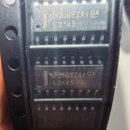
Image for reference only

Manufacturer Part:

SN74LS145DR

Package:

SOIC-16 (D) (9.9 x 6.0 x 1.58 mm, 1.27mm pitch)

Brand:
Product Categories:
Other recommendations you may be interested in.
Description

The SN74LS145DR from Texas Instruments is a BCD-to-decimal decoder/driver in a 16-pin SOIC (D) package with tape and reel packaging. Key specifications: decodes 4-bit BCD input (A, B, C, D) to 1-of-10 active-low outputs (0 through 9); open-collector NPN output transistors with 80 mA sink current capability per output; 15 V output breakdown voltage; all outputs are OFF for invalid BCD input conditions (10-15); low power dissipation 35 mW typical for LS variant; TTL and DTL compatible inputs; compatible for interfacing with most MOS integrated circuits; operates from a single 5 V supply (4.75 V to 5.25 V); operating temperature 0 to +70 degrees C (commercial grade); 16-pin SOIC package (9.9 x 6.0 mm). The device consists of eight inverters and ten four-input NAND gates. The inverters are connected in pairs to make BCD input data available for decoding by the NAND gates. The high-performance NPN output transistors are designed for use as indicator, relay, or open-collector logic-circuit drivers. MSL Level-1-260C-UNLIM. RoHS compliant. Active product status.

The SN74LS145DR from Texas Instruments is a BCD-to-decimal decoder/driver that converts a 4-bit Binary-Coded Decimal (BCD) input into one of ten active-low outputs. It belongs to the venerable 74LS (Low-power Schottky) TTL logic family, which has been a workhorse of digital electronics since the 1970s.

The SN74LS145 is unique among standard logic decoder ICs because it combines decoding with driving capability. Unlike simple decoders such as the 74LS42 (BCD-to-decimal decoder without drive capability), the 74LS145 features high-performance NPN output transistors with 80 mA sink current capability and 15 V breakdown voltage. This makes it suitable for directly driving loads that standard logic outputs cannot handle, such as indicator lamps, relay coils, LEDs, and other medium-current loads.

The device accepts a 4-bit BCD input (D, C, B, A from most significant to least significant) and activates one of ten outputs (0 through 9) corresponding to the input value. The active output is driven LOW (sinking current), while all other outputs are OFF (open-collector, high impedance). For invalid BCD input codes (10 through 15, which are not valid decimal digits), all outputs are OFF, providing a natural blanking function.

The open-collector output configuration is essential for the driving applications this device was designed for. Each output is the collector of an NPN transistor that can sink up to 80 mA when turned on, and withstand up to 15 V when turned off. This allows the outputs to drive loads connected to a voltage higher than the 5 V logic supply, such as 12 V relay coils or 24 V indicator lamps. The open-collector configuration also allows outputs to be wire-ORed for simple logic combining.

The LS (Low-power Schottky) variant dissipates only 35 mW typical, compared to 215 mW for the original 74145 standard TTL variant. This 6x power reduction makes the LS variant practical for modern designs, especially when multiple decoder/driver ICs are used in a system.

The SN74LS145 is one of the few remaining standard logic devices that serves a driving function rather than just a logic function. While CMOS logic families (74HC, 74LVC) have largely replaced TTL for logic functions, the 80 mA sink current and 15 V breakdown voltage of the 74LS145 are not easily replicated by standard CMOS outputs, which typically have only 4-8 mA drive and 5-6 V breakdown. This unique combination of decoding and driving capability keeps the 74LS145 relevant in specific applications.

Common applications include driving 7-segment displays (using two 74LS145 devices in a multiplexed configuration), driving Nixie tube displays (the 15 V breakdown voltage is sufficient for the cathode switching), driving relay banks for sequential control, and driving LED arrays for indicator panels.

The DR suffix denotes the SOIC-16 package with tape and reel (2500 units per reel). The SOIC package is preferred for automated SMT assembly, while the PDIP (N) package is available for prototyping and through-hole applications.

The SN74LS145DR operates as a combinational logic circuit that decodes a 4-bit BCD input into one of ten active-low output signals, using a network of inverters and NAND gates followed by NPN output transistors.

Input Logic: The four BCD input lines (A, B, C, D) represent a decimal digit from 0 to 9. Input A is the least significant bit (LSB) and D is the most significant bit (MSB). The input coding follows standard BCD: 0000 = 0, 0001 = 1, 0010 = 2, …, 1001 = 9. Input codes 1010 through 1111 (decimal 10-15) are invalid BCD values and result in all outputs being OFF.

Decoding Logic: The device consists of eight inverters and ten four-input NAND gates. The four BCD inputs and their complements (generated by the inverter pairs) are connected to the NAND gates in a pattern that implements the BCD decoding truth table. Each NAND gate corresponds to one decimal output (0 through 9) and is wired to activate only when the BCD input matches the corresponding decimal value. For example, the NAND gate for output 0 receives inputs A-complement, B-complement, C-complement, and D-complement, so it activates only when all inputs are LOW (BCD 0000).

Invalid BCD Handling: The NAND gate wiring inherently ensures that none of the ten NAND gates activates for input codes 1010 through 1111. This is because each output NAND gate requires a specific combination of true and complemented inputs that only matches a valid BCD value (0-9). For example, output 0 requires D=0, which is not satisfied for any code 1010-1111 (where D=1). Similarly, outputs 8 and 9 require D=1 with specific ABC patterns that do not match the invalid codes. This full decoding of valid input logic ensures that all outputs are OFF for invalid inputs, providing natural blanking.

Output Stage: Each of the ten outputs is an NPN transistor with an open-collector configuration. When the corresponding NAND gate output is LOW (the selected output), the NAND gate drives the base of the NPN transistor through a current-limiting resistor, turning the transistor ON. The transistor saturates, pulling the output pin LOW (close to GND) and sinking current through the load connected between a positive supply and the output pin. When the NAND gate output is HIGH (unselected outputs), the NPN transistor is OFF and the output pin is effectively open-circuited (high impedance), allowing the load to be pulled to the external supply voltage through the load itself.

Current Drive: Each output transistor can sink up to 80 mA of continuous current. The transistor is designed with a saturated collector-emitter voltage (VCE(sat)) of approximately 0.7 V at 80 mA, so the voltage drop across the output transistor is relatively small even at maximum current. The output breakdown voltage (VCE(off)) is 15 V minimum, meaning the output can be connected to loads powered by up to 15 V when the transistor is OFF.

Power Dissipation: The LS variant uses Schottky-clamped transistors in the internal logic gates, which prevents the transistors from entering deep saturation and reduces storage time. This results in a typical power dissipation of only 35 mW, compared to 215 mW for the standard TTL 74145 variant. The lower power dissipation also reduces the junction temperature rise, improving reliability in multi-IC applications.

TTL Input Characteristics: The inputs are standard LS TTL, requiring 0.4 mA sink current at LOW level (0.8 V maximum) and negligible current at HIGH level (20 uA at 2.7 V minimum). One LS TTL input represents one unit load, so the 74LS145 inputs can be driven by any standard LS TTL output. The inputs are also compatible with CMOS logic (74HC, 74HCT) when appropriate pull-up resistors are used to ensure the HIGH level exceeds the 2 V minimum TTL threshold.

Pin Name Type Description
1 A Input BCD input, least significant bit (LSB); TTL compatible input; represents the 2^0 digit of the BCD code; input current 0.4 mA max at LOW level; connect to BCD counter or logic output; one LS TTL unit load
2 B Input BCD input, second bit; represents the 2^1 digit of the BCD code; same TTL input characteristics as pin A
3 C Input BCD input, third bit; represents the 2^2 digit of the BCD code; same TTL input characteristics as pin A
4 D Input BCD input, most significant bit (MSB); represents the 2^3 digit of the BCD code; same TTL input characteristics as pin A
5 Output 0 Output Active-low open-collector output for decimal digit 0; active (LOW) when BCD input is 0000; sink current up to 80 mA; breakdown voltage 15 V; connect load between positive supply (up to 15 V) and this pin; when inactive, output is OFF (high impedance)
6 Output 1 Output Active-low open-collector output for decimal digit 1; active when BCD input is 0001; same output characteristics as Output 0
7 Output 2 Output Active-low open-collector output for decimal digit 2; active when BCD input is 0010; same output characteristics as Output 0
8 GND Power Ground; 0 V reference; connect to PCB ground plane; provides the ground reference for internal logic and the emitter connection for the output transistors; must carry the total sink current from all active outputs
9 Output 3 Output Active-low open-collector output for decimal digit 3; active when BCD input is 0011
10 Output 4 Output Active-low open-collector output for decimal digit 4; active when BCD input is 0100
11 Output 5 Output Active-low open-collector output for decimal digit 5; active when BCD input is 0101
12 Output 6 Output Active-low open-collector output for decimal digit 6; active when BCD input is 0110
13 Output 7 Output Active-low open-collector output for decimal digit 7; active when BCD input is 0111
14 Output 8 Output Active-low open-collector output for decimal digit 8; active when BCD input is 1000
15 Output 9 Output Active-low open-collector output for decimal digit 9; active when BCD input is 1001
16 VCC Power Positive supply voltage; 5 V nominal (4.75 V to 5.25 V); bypass with 100 nF ceramic capacitor to GND placed close to the pin; the supply powers the internal logic gates; output load current flows through the external load and the output transistor to GND (not through VCC)
Application Description
Relay Driver for Sequential Control Drive up to 10 relays in a sequential control system; BCD counter input selects which relay to activate; 80 mA sink current per output directly drives most 5 V and 12 V relay coils (with flyback diode); 15 V breakdown allows driving 12 V relay coils; only one relay active at a time (1-of-10 decoding); invalid BCD inputs de-energize all relays (safe state)
Indicator Lamp / LED Panel Driver Drive 10 indicator lamps or LED groups on a control panel; each output sinks up to 80 mA (enough for multiple LEDs in parallel with current-limiting resistors); BCD input from counter or microcontroller selects which indicator is lit; open-collector outputs allow LED anodes to be connected to 12 V supply for brighter indicators; low 35 mW power dissipation for the decoder itself
Nixie Tube Cathode Driver Drive the 10 cathodes (digits 0-9) of a Nixie tube; open-collector outputs with 15 V breakdown can withstand the Nixie tube cathode voltage when OFF; BCD input from counter selects which digit illuminates; each output only needs to sink the Nixie tube operating current (2-5 mA typical), well within the 80 mA rating; requires anode supply resistor to limit current
Decimal Display Multiplexing Use two 74LS145 devices with a BCD counter and multiplexing circuit to drive a multi-digit 7-segment display; one 74LS145 drives the digit select lines (via PNP transistors for digit anodes) while another decodes segment data; the 80 mA sink capability drives the segment current directly for small displays; reduces component count compared to discrete transistor drivers
Solenoid Valve Driver Drive up to 10 solenoid valves in industrial control systems; BCD input selects which valve to open; 80 mA sink current handles small solenoid valves directly; larger solenoids require external driver transistors (74LS145 output drives the base of an external NPN); 15 V breakdown allows 12 V solenoid supply; invalid BCD ensures all valves closed for safety
Model Manufacturer Compatibility Key Difference
SN74LS145N TI Same Die, Different Package Same BCD-to-decimal decoder/driver in PDIP-16 package; through-hole mounting; same electrical specifications and pinout; use for prototyping and through-hole PCB designs; different package only; larger footprint (19.3 x 9.4 mm vs 9.9 x 6.0 mm)
SN74145N TI Original TTL, Higher Power Original standard TTL version; same BCD-to-decimal function; same 80 mA output sink capability; same pinout; much higher power dissipation (215 mW vs 35 mW typical); use only as replacement in legacy standard TTL designs; not recommended for new designs
SN74LS42 TI Decoder Only, No Drive BCD-to-decimal decoder (1-of-10) without the high-current output drivers; standard totem-pole outputs (0.4 mA sink); does not have open-collector 80 mA drivers; cannot directly drive lamps, relays, or high-current loads; use when only logic-level decoding is needed and external drivers are used for load switching
CD4028B TI CMOS Alternative BCD-to-decimal decoder in CMOS (CD4000 series); 16-pin DIP or SOIC; standard CMOS outputs (not high-current); wider supply voltage range (3-15 V); much lower output drive (1 mA at 10 V); lower power consumption; use for low-power CMOS designs that do not need the 80 mA drive capability
ULN2803A TI/ST Darlington Driver Array 8-channel Darlington transistor array; 500 mA per channel sink current; not a decoder (requires external BCD decoding logic); much higher drive current; built-in flyback diodes for inductive loads; use when driving high-current loads that exceed the 74LS145 80 mA rating; must be combined with a separate BCD decoder
Recommend Parts
HDMI 2.0 Bridge, 4K@60Hz, HDCP 2.2 Repeater, MHL 3.0, 76-pin QFN EP

Brand:

Package:

76-Pin QFN EP (9.0 x 9.0 x 0.83 mm)
In stock:
6848pcs

Cargo cycle: 3~7 Days
The minimum order is 1

Go to Inquiry
4700pF 3000V X7R MLCC, 10%, 1812, high-voltage TANCERAM, -55 to 125C, tape and reel

Brand:

Package:

1812 (4.50 x 3.18 x 2.80 mm)
In stock:
4146pcs

Cargo cycle: 3~7 Days
The minimum order is 1

Go to Inquiry
N-Channel depletion-mode MOSFET, 1000V, 10A, 1.5Ohm, normally-on, TO-268AA, 695W

Brand:

Package:

TO-268AA / D3PAK (15.75 x 13.08 x 4.83 mm)
In stock:
14959pcs

Cargo cycle: 3~7 Days
The minimum order is 1

Go to Inquiry
16Mbit SPI NOR Flash, 3V, QSPI/QPI, 133MHz, DTR, SOIC-8 150mil, -40 to 105C, TR

Brand:

Package:

8-SOIC (4.90 x 3.90 x 1.75 mm, 150mil)
In stock:
11082pcs

Cargo cycle: 3~7 Days
The minimum order is 1

Go to Inquiry
256Mbit SPI NOR Flash, 1.8V, QPI/QSPI, 104MHz, DTR, WSON-8 6x8mm, -40 to 105C

Brand:

Package:

8-WSON (6.0 x 8.0 x 0.73 mm, exposed pad)
In stock:
13368pcs

Cargo cycle: 3~7 Days
The minimum order is 1

Go to Inquiry
8Mbit async SRAM, 512Kx16, 2.5-3.6V, 55ns, ultra-low power, 48-mini BGA, Industrial

Brand:

Package:

48-Mini BGA (7.2 x 8.7 x 0.9 mm)
In stock:
3838pcs

Cargo cycle: 3~7 Days
The minimum order is 1

Go to Inquiry
Quality Assurance

Quality is the core foundation of our long-term global cooperation. With over 20 years of experience in the electronic component industry, Materialparts has built a strict and standardized quality management system covering component sourcing, incoming inspection, full-batch testing, packaging and delivery. We are committed to delivering 100% genuine, high-reliability electronic components for industrial control, automotive electronics, consumer electronics and medical device industries, and fully safeguarding your production and R&D projects.

1. Authorized & Genuine Sourcing Promise

All of our electronic components are procured from official authorized distributors and original manufacturers. We strictly reject counterfeits, refurbished parts, disassembled components and gray-market goods. Every product is guaranteed to be brand-new original parts and fully consistent with the original technical parameters. For branded products such as NXP IC series, we maintain complete supply channel documents to realize full product traceability.

2. Strict Full-batch Quality Inspection

We implement 100% full-batch quality control for all goods before shipment. Our professional QC team conducts multi-dimensional tests including appearance inspection, electrical parameter testing, performance verification and packaging check. Each batch of components is attached with complete inspection reports and batch records. We stick to zero-tolerance standards for defective products to ensure every piece of component meets industrial application requirements.

3. Industry Standard Compliance

Our products comply with a variety of international industry quality standards to adapt to high-standard application scenarios:
  • Automotive Electronics: All automotive-grade components pass AEC-Q series certification, featuring excellent stability and durability to adapt to complex vehicle operating environments.
  • Medical Devices: High-reliability components meet medical industry safety and compliance regulations, ensuring stable operation for medical equipment.
  • Industrial Control & Consumer Electronics: Products conform to universal international electronic industry standards, suitable for long-term continuous operation of various equipment.

4. Professional Reliability Control

For static-sensitive, moisture-sensitive and precision components such as ICs, PCBs, sensors and connectors, we carry out reliability screening in advance. Combined with standardized ESD anti-static packaging and vacuum moisture-proof packaging, we avoid component damage caused by static electricity, dampness or collision during storage and transportation, and retain the original performance of products.

5. Traceability Management System

We establish a complete product traceability system. Each batch of goods corresponds to independent batch number, sourcing record, inspection record and delivery record. Customers can query the whole lifecycle information of components at any time. This system effectively solves quality risks and facilitates after-sales handling and production quality control for your company.

6. After-sales Quality Guarantee

If any product is confirmed to have non-conformity quality problems due to our reasons after receipt, we provide free return, exchange and supplementary delivery services. Our professional quality team will also conduct root cause analysis to optimize our quality control process. We respond to quality feedback within 24 hours to resolve your worries efficiently.

Contact Us

If you have inquiries about our quality standards, inspection procedures or product certification documents, please feel free to contact us:


Email: info@materialparts.com
Tel / WhatsApp: +86 13760382860
Address: Room 2919, Guoli Building, Huaqiang North, Futian District, Shenzhen, Guangdong, China


Shipping & Payment

Materialparts is a professional global supplier of electronic components with over 20 years of industry experience. We provide one-stop supply of passive components, integrated circuits, as well as parts for industrial control, automotive electronics, consumer electronics and medical devices. Below are the unified shipping and payment policies applicable to all orders, samples and bulk purchases worldwide.

1. Payment Terms

We offer a variety of secure and convenient payment methods to meet diverse business cooperation needs. Details are as follows:
  1. Accepted Payment Methods
  • T/T (Bank Wire Transfer): The primary settlement method for bulk orders and a widely used international payment channel.
  • PayPal: Ideal for small orders, sample orders and quick payments.
  1. Settlement Currency


    US Dollar (USD) is the default settlement currency. RMB is available for domestic customers.

  2. Bank Charges


    All transfer fees, intermediary bank charges and other remittance-related expenses shall be borne by the buyer.

  3. Payment Requirements
  • Sample and small orders: Shipment will be arranged upon full payment.
  • In-stock bulk orders: Goods will be delivered within 2 to 3 working days after full payment.

2. Shipping & Delivery

We partner with leading global logistics providers to ensure safe and fast delivery worldwide. Relevant details are listed below:
  1. Logistics Partners
  • International Express: DHL, FedEx, UPS, TNT
  • Economy Logistics: Air freight and sea freight for large-volume cargo
  • Domestic Delivery: SF Express, Yunda Express
  1. Order Processing Time
  • In-stock items: Orders confirmed and fully paid before 14:00 (GMT+8) will be shipped on the same day. All other orders will be dispatched within 1 to 2 working days.
  • Out-of-stock or sourced items: The delivery lead time will be confirmed separately according to brand and inventory status.
  1. Estimated Transit Time
  • International Express: 3 – 7 working days globally
  • Air Freight: 7 – 12 working days
  • Sea Freight: 25 – 40 working days for heavy and large bulk cargo
  1. Shipping Fee Rules
  • Shipping cost is calculated based on package weight, volume, destination and delivery method.
  • Both freight prepaid and freight collect are available. Please provide your courier account number in advance if you choose freight collect.
  • Free international express delivery is offered for large orders. Terms for long-term partners can be negotiated separately.
  1. Shipment Tracking
     

    Within 24 hours after dispatch, we will send the tracking number, commercial invoice, packing list and other documents to your email or communication account. You may check the shipment status online in real time.

3. General Order Rules & Notes

  1. MOQ & Sample Service


    We support flexible minimum order quantities for samples, small-batch and large-batch orders. All sample orders shall comply with the above shipping and payment policies.

  2. Packaging Standard


    All electronic components are packed with professional anti-static and shockproof materials. Original factory packaging is available for branded chips and integrated circuits.

4. Customs & Liability Statement

  1. Import Duties & Taxes


    All import duties, customs clearance fees and local taxes incurred for international shipments shall be borne by the buyer. We will provide complete customs documents to assist you with clearance procedures.

  2. Handling of Lost or Damaged Goods
  • In case of loss or severe damage during transit, please contact us within 48 hours after receiving the tracking information. We will assist you in filing a claim with the logistics provider.
  • We shall not be liable for any losses caused by incorrect delivery address, wrong contact information or the buyer’s refusal to complete customs clearance.

5. Local Pickup in Shenzhen

Local pickup service is available for customers in Shenzhen and surrounding areas:
  • Address: Room 2919, Guoli Building, Huaqiang North, Futian District, Shenzhen, Guangdong Province, China
  • Business Hours: 09:00 – 18:00, Monday to Friday. Closed on weekends and official public holidays.
  • Notice: Please make an appointment via email or communication tools one day in advance, and present your order information upon pickup.

Contact Information

Email: info@materialparts.com

Tel / WhatsApp: +86 13760382860

Service & Packaging

Materialparts is a professional electronic component supplier based in Shenzhen, China, with over 20 years of global trading experience. We integrate component procurement, quality inspection, technical support, customized packaging, and global delivery services to provide one-stop supply chain solutions. Our business covers industrial control, automotive electronics, consumer electronics, medical devices and other industries. We always adhere to genuine sources, stable supply and considerate after-sales service.

Core Services

1. One-stop Sourcing & BOM Support

We specialize in a full range of passive and active electronic components, including SMD resistors, power resistors, connectors, aviation connectors, LED beads, flexible circuit boards, printed circuit boards, and integrated circuits. Our professional team provides BOM list consolidation, component matching, and alternative model recommendation services. We support sample orders, small-batch trial production, and mass production orders with flexible MOQs to meet diverse procurement needs.

2. Genuine Product Guarantee & Full-process Quality Inspection

All products are sourced from official authorized channels and are 100% original genuine parts. Every batch of goods undergoes strict full-process quality inspection before delivery, with complete batch records and traceability documents provided. Our products comply with AEC-Q standards for automotive electronics and high-reliability specifications for medical devices. We eliminate counterfeits, refurbished parts and defective products from the source to secure your project production.

3. Fast Quotation & Order Processing

Our customer service team responds promptly to inquiries and quotation requests. All in-stock orders will be processed within one working day. We provide stocking reservation services for long-term cooperative customers, effectively solving problems such as component shortages and unstable supply chains.

4. Professional Technical Support

Our senior engineer team provides free technical consultation, model selection guidance and original manufacturer datasheets. We assist customers in solving problems related to product R&D, circuit design and component application, providing reliable technical support for project progress.

5. Sourcing for Special Components

Relying on our global supply chain network, we professionally source scarce components, obsolete parts and customized special components to efficiently solve your procurement difficulties.

6. Global Logistics & Document Services

We cooperate with mainstream international logistics providers including DHL, FedEx, UPS and TNT to achieve fast global delivery. We can provide complete export documents such as customs declaration files, commercial invoices and packing lists to ensure smooth customs clearance for international shipments. Local pickup is also available for customers in Shenzhen, China.

Professional Packaging Standards

Electronic components are sensitive to static electricity, collision, moisture and dust. We adopt industry-standard anti-static packaging solutions to fully ensure the integrity of goods during transportation and storage.

1. General Packaging Specifications

  • All components are packed separately to avoid damage caused by friction and collision;
  • Shockproof buffer materials are added for fragile products to ensure transportation safety;
  • Each package is clearly marked with part number, quantity, batch number and specifications for easy inventory counting and management.

2. Classified Professional Packaging

  • Anti-static Packaging: Static-sensitive components such as chips, circuit boards and sensors are packaged with anti-static bags, shielding boxes and conductive foam in strict accordance with international anti-static standards to prevent static damage.
  • Vacuum Moisture-proof Packaging: Moisture-sensitive components are vacuum-sealed with desiccants to isolate humid air, suitable for ocean transportation and long-term storage.
  • Original Factory Packaging: Integrated circuits of brands such as NXP are delivered with original reels, trays or tubes by default, retaining complete original packaging and adapting to automated SMT production lines.
  • Discrete Device Packaging: Discrete devices such as SMD resistors, power resistors and LEDs are quantitatively and classifiedly packaged with accurate quantity and clear marking.
  • Connector / Aviation Connector Packaging: Hard outer packaging is adopted to prevent pin bending and structural deformation.

3. Custom Packaging Services

We provide value-added services including personalized packaging, custom labeling and re-reeling according to customer requirements, fully matching your production and warehouse management standards.

Contact Information

For service consultation or packaging customization, please feel free to contact us:
Email: info@materialparts.com
Tel / WhatsApp: +86 13760382860
Address: Room 2919, Guoli Building, Huaqiang North, Futian District, Shenzhen, Guangdong, China
 

Online Inquiry Form

Support Excel, PDF, CSV format files for full BOM list quotation

Submit your component procurement and custom packaging needs via the form below. We will provide a detailed quotation and professional solution within 1–8 working hours.



