
Introduction / Industry Overview
Instruments and meters represent the precision end of the electronic manufacturing spectrum—where the difference between a competent product and a superior one is measured in parts per million. Whether the application is a benchtop digital multimeter, a field-calibration instrument for process control, a vibration data acquisition system, or a laboratory power analyzer, the PCB is the primary determinant of measurement accuracy, long-term stability, and calibration integrity.
The global test and measurement equipment market was valued at approximately USD 32 billion in 2025, projected to reach USD 48 billion by 2030 at a CAGR of 7.0% (Grand View Research, 2025). Within this market, the PCB’s contribution to instrument performance is often underappreciated: trace impedance variations affect ADC reference accuracy, thermal gradients across voltage references introduce drift, and parasitic capacitance on analog input traces degrades signal-to-noise ratio. In precision instrumentation, the PCB is not merely a substrate—it is a calibrated component of the measurement system.
This article examines the core technologies, application cases, and future trends shaping instruments and meters PCB design, with emphasis on calibration strategies, low-noise analog design, and the standards that define measurement integrity.
Core Technology Analysis
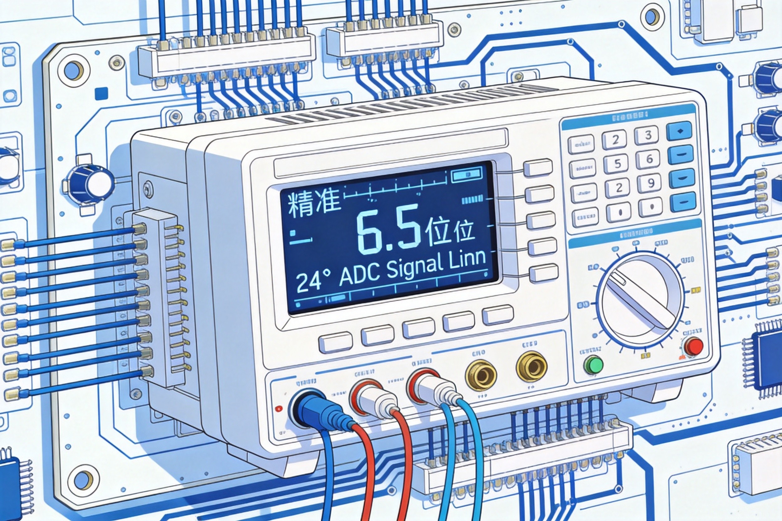
Precision Calibration Architecture: Hardware Self-Correction
The defining challenge of precision instrumentation is maintaining accuracy over time, temperature, and environmental exposure. A digital multimeter that reads 0.005% accuracy at calibration may drift to 0.012% after six months of field use if the PCB lacks proper calibration architecture. The solution is hardware self-calibration—integrating reference elements directly onto the PCB that enable the instrument to periodically correct its own measurement errors.
Voltage Calibration: A high-precision voltage reference such as the ADI ADR4550 (5.000 V output, ±0.001% initial accuracy, temperature coefficient ≤1 ppm/°C) is integrated into the measurement chain. The MCU periodically switches the ADC input from the measurement signal to the reference voltage, measures any deviation from the expected value, and calculates correction coefficients. A documented case: a precision multimeter without hardware calibration drifted from 0.005% to 0.012% error over 6 months; after integrating the ADR4550 with auto-calibration logic, the error remained stable at 0.004–0.006% over 12 months.
Current Calibration: Standard current sources (e.g., LTC6078, 100 nA–1 mA, ±0.005% accuracy) calibrate the sampling resistor’s value偏差. If the sampling resistor drifts by 0.005% annually, post-calibration error can be corrected to 0.001%.
Impedance Calibration: Low-temperature-coefficient standard resistors (Vishay Z-Foil, temperature coefficient ≤0.05 ppm/°C) and standard capacitors (AVX C0G, ±3 ppm/°C) serve as on-board references for impedance measurement chains.
Calibration Control Logic: The MCU or FPGA manages the calibration cycle (e.g., hourly auto-calibration or pre-measurement manual trigger), stores correction coefficients in EEPROM (e.g., Microchip 24LC02, 1 million erase/write cycles), and applies them in real time during every measurement. Calibration duration is typically ≤100 ms, ensuring minimal interruption to the measurement process.
Low-Noise Analog Signal Chain Design
Precision instruments must capture signals ranging from nanovolts (thermocouple outputs) to hundreds of volts (power line measurements) with 24-bit ADC resolution. The analog signal chain—from input connector through protection, filtering, amplification, and ADC conversion—demands obsessive attention to noise, linearity, and drift.
ADC Selection and PCB Integration: Modern 24-bit delta-sigma ADCs offer remarkable performance. Key devices include:
| ADC | Resolution | Max Sample Rate | Input-Referred Noise | Key Feature |
|---|---|---|---|---|
| TI ADS1256 | 24 bit | 30 kSPS | 27 nV (PGA = 64) | Chopper-stabilized input buffer, 8-channel MUX |
| TI ADS124S08 | 24 bit | 4 kSPS | 19 nV (PGA = 128) | 12-channel MUX, integrated IDACs for RTD biasing |
| ADI AD7172-2 | 24 bit | 31.25 kSPS | 24 noise-free bits @ 5 SPS | True rail-to-rail buffers, 2 ppm/°C internal reference |
| ADI MAX11216 | 24 bit | 64 kSPS | 6.5 nV/√Hz (PGA) | 140 dB SNR, 1 ppm INL, 10 mW power |
The PCB design rules for achieving specified ADC performance are stringent:
-
Voltage reference routing: The ADC’s reference input traces must be routed as a Kelvin-connected differential pair, with guard traces connected to the reference ground. Any voltage drop along the reference trace directly introduces gain error. For a 2.5 V reference with 1 ppm accuracy requirement, a 2.5 μV drop (equivalent to 0.1 Ω trace resistance carrying 25 μA of reference input current) consumes the entire error budget.
-
Analog ground plane integrity: The ADC’s analog ground must be connected to the system ground at a single point—typically the ADC’s ground pin—through a short, wide trace. Digital ground currents from the SPI interface must flow through a separate ground path to prevent switching noise from modulating the analog reference.
-
Clock isolation: The ADC’s clock source (crystal oscillator or external clock) must be physically separated from the analog input section. Clock harmonics coupling into the analog front end create spurious tones in the ADC output spectrum. A ground-plane slot between the clock section and the analog section, with the slot bridged only at the ADC ground pin, is an effective isolation strategy.
-
Power supply sequencing: The ADC’s analog supply must be stable before the digital supply is applied, and the reference voltage must be settled before the first conversion. Reverse sequencing can cause latch-up or reference damage. The PCB power supply design must enforce the correct start-up order through voltage supervisors or sequencer ICs.
Drift Control: Temperature, Humidity, and Time
Temperature Drift Management: A 1°C temperature change causes PCB substrate dielectric constant variation, component parameter shifts, and thermocouple effects at dissimilar metal junctions (copper traces to component leads). The target is to limit temperature-induced drift to ≤0.001%/°C:
-
Substrate selection: Standard FR-4 has a dielectric constant temperature coefficient ≥10 ppm/°C. Rogers RO4350B reduces this to ≤3 ppm/°C—a 70% improvement. For the most demanding applications, polyimide or PTFE substrates offer temperature coefficients below 1 ppm/°C.
-
Temperature monitoring and compensation: High-precision temperature sensors (e.g., NXP NTCG104ED104F, ±0.1°C at 25°C) are placed at critical PCB locations (ADC, voltage reference, input conditioning). The MCU executes compensation algorithms based on measured temperature, correcting for known drift characteristics of each component.
-
Thermal symmetry: Components that must track each other (such as differential input resistors in a Wheatstone bridge measurement) must be placed symmetrically with respect to heat sources, ensuring that temperature gradients affect both elements equally and the differential measurement cancels the common-mode error.
Humidity Drift: A 10% RH change can cause 0.005% capacitance parameter shift on uncoated FR-4. Solutions include:
-
Low-absorption conformal coating: Dow Corning DC1-2577 (water absorption ≤0.1%), applied at 20–30 μm thickness, reduces humidity-induced capacitance drift from 0.005% to 0.001% per 10% RH change.
-
Humidity monitoring: Sensirion SHT31 (±2% RH accuracy) enables software compensation for residual humidity effects.
Long-Term (Aging) Drift: Component aging causes parameter shifts over years of operation. The target is annual drift ≤0.005%:
- Resistor selection: Vishay Z-Foil metal foil resistors exhibit annual drift ≤0.0005%, versus ≥0.01% for metal film resistors.
- Capacitor selection: NP0/C0G MLCCs (TDK CGA series) have annual drift ≤0.001%, versus ≥1% for aluminum electrolytics.
- Amplifier selection: Chopper-stabilized op-amps (e.g., ADI OP27, input offset drift ≤0.2 μV/°C) eliminate the 1/f noise and drift that plague standard precision amplifiers.
Standards Compliance: IEC 61298 and IEC 60751
Instruments and meters must comply with a framework of standards that define measurement accuracy, environmental performance, and safety:
-
IEC 61298 (Process measurement and control devices): Defines general methods for evaluating the performance of process measurement and control devices, including accuracy, repeatability, dead band, and environmental influence tests (temperature, humidity, vibration, electromagnetic interference).
-
IEC 60751 (Industrial platinum resistance thermometers): Specifies the resistance/temperature relationship and tolerance classes for Pt100/Pt1000 RTDs. Class AA RTDs require ±(0.1 + 0.0017|t|)°C accuracy, demanding PCB-level thermal management to prevent self-heating errors from the excitation current.
-
ISO/IEC 17025 (Calibration laboratory competence): Instruments used as calibration references must maintain traceability to SI units through NIST or equivalent national standards. Annual recalibration per ISO 10012-1 is standard practice, with back-to-back comparison against reference standards.
-
IEC 61010-1 (Safety requirements for electrical equipment for measurement, control, and laboratory use): Defines creepage and clearance distances, insulation requirements, and protective measures for instruments operating at hazardous voltages.
Typical Application Cases

Case 1: 6.5-Digit Digital Multimeter — Sub-PPM Accuracy
A 6.5-digit benchtop digital multimeter must resolve 100 nV on the 100 mV range and maintain 24-hour accuracy of ±(0.002% of reading + 0.0005% of range) after calibration.
PCB Design Approach: 8-layer FR-4 with dedicated analog and digital ground planes. The ADC section uses the ADI AD7172-2 (24 noise-free bits at 5 SPS) with an external ADR4550 voltage reference. The analog input path includes a chopper-stabilized preamplifier (ADI ADA4522-2, 5.6 nV/√Hz input noise, 0.01 μV/°C offset drift) followed by a programmable gain stage. All critical resistors are Vishay Z-Foil types with ≤0.05 ppm/°C temperature coefficients. The input protection network (spark gaps, TVS diodes, PTC fuses) is physically isolated from the measurement section by a ground-plane slot. Auto-calibration runs every hour, switching the ADC input through internal reference voltages and a precision resistor network to correct gain and offset errors.
Result: 24-hour accuracy of ±(0.0018% + 0.0004%), 90-day accuracy of ±(0.004% + 0.0006%), and temperature coefficient of 0.0005%/°C—meeting the manufacturer’s specification for a 6.5-digit instrument.
Case 2: Process Calibrator — HART Communication and 4–20 mA Loop Testing
A handheld process calibrator must source and measure 4–20 mA current loops with 0.01% accuracy while simultaneously communicating with HART (Highway Addressable Remote Transducer) field devices.
PCB Design Approach: 6-layer board with the current source/sink circuit (using a precision Howland current pump with Vishay Z-Foil set resistors) on one side and the HART modem (using a dedicated FSK modulation/demodulation IC) on the other, separated by a ground-plane partition. The current loop output uses a 4-wire Kelvin sense configuration to eliminate lead resistance errors. The HART modem’s 1200/2200 Hz FSK signals are transformer-coupled into the current loop, with bandpass filtering to prevent the HART tones from affecting the DC current accuracy. A precision 250 Ω shunt resistor (0.01% tolerance, 2 ppm/°C drift) converts the loop current to a voltage measured by the ADS124S08 ADC.
Result: Current accuracy of ±0.01% of reading, HART communication success rate >99.9%, and battery life exceeding 20 hours from a 7.4 V Li-ion pack.
Case 3: Vibration Data Acquisition System — 24-Bit Wideband Measurement
A 4-channel vibration data acquisition system must capture accelerometer signals from 0.5 Hz to 54 kHz with >105 dB dynamic range, for predictive maintenance of rotating machinery.
PCB Design Approach: Each channel uses a continuous-time delta-sigma ADC (ADI AD4134) with 24-bit resolution at up to 375 kSPS, preceded by a charge amplifier for IEPE/ICP piezoelectric accelerometers (2–20 pF sensor capacitance, 4 mA constant-current excitation). The charge amplifier uses a low-noise JFET-input op-amp (ADI AD8065, 6.6 nV/√Hz) with a 1 GΩ feedback resistor and low-leakage polypropylene feedback capacitor. The ADC’s SPI data lines are routed as impedance-controlled differential pairs to the FPGA, with source-synchronous clocking to eliminate timing skew between channels. Power for the analog section is provided by ultra-low-noise LDO regulators (LT3042, 0.8 μV RMS output noise over 10 Hz–100 kHz).
Result: Dynamic range of 105.9 dB with shorted input at 64 kSPS, channel-to-channel phase matching within 0.1°, and total harmonic distortion below −110 dB—matching the performance of piezoelectric reference accelerometers such as the PCB Piezotronics Model 621B40.
Future Development Trends
AI-Enhanced Calibration and Self-Optimizing Instruments
Machine learning algorithms are being integrated into precision instruments to move beyond fixed calibration tables toward adaptive, predictive calibration. By monitoring drift trends across temperature, humidity, and operating time, AI models can predict when the next recalibration is needed and dynamically adjust correction coefficients between scheduled calibrations. This approach can extend the calibration interval from 12 months to 24+ months for instruments in stable environments, while flagging instruments in harsh conditions that need more frequent attention. Timeframe: AI-enhanced calibration is in prototype (2025–2026); mainstream adoption in premium instruments expected by 2028–2029.
Multi-Channel Synchronized Data Acquisition
The demand for structural health monitoring, power quality analysis, and vibration-based predictive maintenance is driving instruments toward higher channel counts with tighter synchronization. The ADI AD4134’s continuous-time architecture eliminates the need for external anti-aliasing filters, simplifying multi-channel PCB design, while deterministic SPI interfaces and FPGA-based time-stamping achieve inter-channel synchronization below 10 ns. Instruments with 8–64 synchronized channels at 24-bit resolution are becoming standard for power grid monitoring and seismic data acquisition. Timeframe: 8–16 channel instruments are in production now; 32–64 channel systems at 24-bit resolution will be mainstream by 2027–2028.
Wireless Calibration and Cloud-Connected Metrology
The convergence of precision measurement with IoT connectivity is enabling remote calibration verification and cloud-based metrology data management. Instruments with built-in Wi-Fi or Bluetooth LE can upload measurement data and calibration status to cloud platforms, where AI algorithms detect drift patterns and trigger recalibration alerts. This eliminates the need for physical recalibration visits in many cases and enables fleet-wide calibration management for large industrial installations. PCB designers must accommodate wireless modules alongside ultra-sensitive analog circuits—a co-design challenge requiring careful RF-analog isolation. Timeframe: Cloud-connected calibrators are available now; fully automated remote recalibration will emerge by 2028–2029 as regulatory frameworks (ISO/IEC 17025 digital calibration certificates) mature.
Conclusion
Instruments and meters PCB design is a discipline where the pursuit of accuracy is measured in parts per million and every design decision—from reference voltage routing to conformal coating selection—has a direct, quantifiable impact on measurement performance. The integration of hardware self-calibration, ultra-low-noise ADC signal chains, and comprehensive drift control strategies enables modern instruments to maintain sub-ppm accuracy over years of field operation. As the industry moves toward AI-enhanced calibration, multi-channel synchronized acquisition, and cloud-connected metrology, the PCB designer’s role is expanding from analog circuit layout to system-level precision engineering. For electronics manufacturers competing in the test and measurement market, the ability to deliver PCBs that preserve calibration integrity from the laboratory to the factory floor is the foundation of customer trust and market differentiation.
Need precision instrument PCB manufacturing with calibration-grade reliability? Connect with our engineering team to discuss low-noise design strategies and IEC 61298-compliant manufacturing capabilities.
 English
  简体中文
简体中文  Español
  العربية