
Introduction / Industry Overview
The security and surveillance industry has undergone a structural transformation—from analog CCTV systems where the PCB’s primary job was signal conditioning and video encoding, to AI-powered intelligent systems where the PCB must simultaneously process multiple 4K video streams, run neural network inference, and maintain encrypted network connectivity in environments that range from climate-controlled server rooms to desert-mounted camera poles. The global video surveillance market was valued at approximately USD 58 billion in 2025, projected to reach USD 120 billion by 2030 (MarketsandMarkets, 2025), driven by smart city initiatives, critical infrastructure protection, and the rapidly expanding demand for AI-driven analytics.
This transformation has fundamentally changed PCB design requirements. A modern AI-enabled surveillance camera contains an SoC with integrated NPU (neural processing unit), multi-gigabit high-speed interfaces for image sensors, hardware-accelerated H.265 encoding, Power-over-Ethernet (PoE) power management, and encrypted secure-boot firmware—all on a PCB that must operate reliably at −30°C to +60°C in outdoor housings with limited passive cooling. The PCB is no longer a passive interconnect; it is the computational substrate of an intelligent edge device.
This article examines the core technologies, application cases, and future trajectory of security and surveillance PCB design, with emphasis on AI edge computing integration, multi-sensor camera architectures, and cybersecurity compliance.
Core Technology Analysis

AI Edge Computing Integration: NPU SoC PCB Design
The transition from cloud-centric to edge-centric AI processing is the defining technical shift in surveillance PCB design. Sending all video streams to cloud servers for analysis is unsustainable at scale: a 200-camera deployment at 1080p/30fps generates over 2 Tbps of raw data—far exceeding practical upload bandwidth. The solution is AI inference at the edge, where the camera or a local gateway runs neural network models (object detection, behavior analysis, anomaly detection) on-device.
Key SoC Platforms and PCB Implications:
| SoC Platform | AI Performance | Video Capability | PCB Design Impact |
|---|---|---|---|
| Rockchip RK3588 | 6 TOPS (INT8) | 8K@60fps decode, 4K@60fps encode | 4×Cortex-A76 + 4×Cortex-A55, LPDDR4X 4-ch, PCIe 3.0, requires 6–8 layer HDI, thermal management for ~5W active |
| NVIDIA Jetson Orin NX | 100 TOPS (INT8) | 4K@60fps encode, 8× 4K decode | 8-core Arm A78AE, LPDDR5, requires 10+ layer board, active cooling, 15–25W TDP |
| Ambarella CV2FS | 2.2 TOPS (CNN) | 4K@60fps encode, 4K pipeline | CVflow architecture, dual-core A9, optimized for camera module integration, 1.5–2W |
| Hailo-8 | 26 TOPS (INT8) | N/A (accelerator only) | PCIe/NM/USB interface, 2.5W typical, can be added to existing camera PCB designs as co-processor |
RK3588 PCB Design Example: The Rockchip RK3588, widely adopted in Chinese surveillance equipment, integrates a tri-core NPU, 4800 MP ISP 3.0 (with 2D/3D noise reduction, wide dynamic range, and de-haze processing), and fourth-generation video codec hardware. For a 4-camera AI gateway application, each video frame requires ~15 ms decode time and 30–200 ms AI inference time, enabling real-time processing at ~20 fps across all four channels. The PCB must support:
- LPDDR4X memory interface: 4-channel, 3200 MHz data rate, with strict length matching (±0.1 mm per byte lane) and 100Ω differential impedance
- Multi-camera interface: MIPI CSI-2 (4-lane per camera, 2.5 Gbps per lane) or GigE Vision for network cameras, requiring controlled-impedance routing and ESD protection at each connector
- Thermal management: ~5W active power dissipation in a fanless enclosure requires a copper coin or thermal pad connecting the SoC to an aluminum housing, with thermal interface material (TIM) rated for −40°C to +100°C
- Power delivery: Multiple voltage rails (0.8V core, 0.9V NPU, 1.8V IO, 3.3V peripheral) with dedicated PMIC, each requiring local decoupling and load-switch isolation
IP Camera PCB Architecture: From Sensor to Network
A modern IP camera PCB integrates five functional domains on a single board:
-
Image sensor interface: MIPI CSI-2 (2–4 lanes) connecting the CMOS sensor to the SoC’s ISP, with impedance-controlled differential pairs (100Ω ±5%) and length matching within ±0.2 mm. The sensor itself is mounted on a separate flex PCB that plugs into the main board via a 40–60 pin FPC connector.
-
Video processing and encoding: The SoC’s hardware encoder generates H.265 (HEVC) streams at 4K/30fps, requiring real-time DMA access to LPDDR memory. The memory bus must be routed with length-matched, impedance-controlled traces on inner layers adjacent to solid ground planes.
-
Network interface: Gigabit Ethernet with IEEE 802.3at PoE (Power over Ethernet, 25.5W class). The PoE section includes a powered device (PD) controller, isolated DC-DC converter (48V to 5V/12V), and Ethernet transformer/magnetics with 1500 Vrms isolation. The network section must be physically separated from the analog video section to prevent EMI coupling.
-
IR illumination control: For night-vision capability, the PCB includes an IR-cut filter driver (dual-coil or stepper motor), IR LED current drivers (typically 850nm or 940nm, 1–3W total), and an ambient light sensor (ALS) for automatic day/night switching. The IR LED drivers generate significant switching noise and must be isolated from the image sensor’s analog front end.
-
Secure element and firmware protection: A hardware secure element (e.g., Microchip ATECC608B) provides secure boot, encrypted firmware storage, TLS certificate management, and device authentication—critical for preventing unauthorized firmware modification and network intrusion.
Network Video Recorder (NVR) PCB: High-Density Storage and Multi-Stream Processing
An NVR must simultaneously record and manage 16–128 video streams while providing real-time playback, search, and AI analytics. The PCB challenges center on high-speed memory interfaces, mass storage connectivity, and thermal management.
Storage Interface Design: Modern NVRs use NVMe SSDs (PCIe 3.0 ×4, 4 GB/s) for high-speed recording and HDD arrays (SATA III, 6 Gbps) for archival storage. PCIe traces require 85Ω ±5% differential impedance (per PCIe CEM specification), with length matching within ±0.1 mm and AC coupling capacitors placed within 100 mils of the transmitter pins. SATA traces require 100Ω ±5% differential impedance with similar matching tolerances.
Memory Architecture: Dual-channel DDR4 at 3200 MHz or LPDDR5 for the main processor, with additional DDR4 for the AI inference engine. Total memory bandwidth must exceed 25 GB/s for 32-channel 4K recording. Memory routing occupies a significant fraction of the PCB layer count and demands rigorous signal integrity simulation.
Thermal Design: A 32-channel NVR may dissipate 40–60W across the main SoC, AI accelerator, and storage controllers. The PCB uses 2 oz copper on inner power/ground layers for thermal spreading, with thermal via arrays under each high-power IC. The enclosure design integrates forced-air cooling with dust-filtered intakes, and the PCB must support fan-control temperature monitoring (NTC thermistors at 3–4 locations).
Cybersecurity in PCB Design: Hardware Roots of Trust
Surveillance devices are high-value targets for network intrusion—a compromised camera can provide unauthorized access to video feeds, serve as a pivot point for lateral network movement, or be recruited into a botnet. Hardware-level security measures on the PCB include:
-
Secure boot chain: ROM-based bootloader verifies the first-stage bootloader using RSA-4096 or ECDSA signatures stored in the secure element, which then verifies the OS kernel, which verifies application code. The entire chain must be implemented with hardware-enforced trust anchors that cannot be modified by software.
-
Hardware-encrypted storage: AES-256 hardware encryption for all stored video data, with encryption keys stored exclusively in the secure element—never in application-accessible memory. The PCB must ensure that the secure element’s communication bus (I2C or SPI) is not exposed on test points or debug headers.
-
JTAG/SWD protection: Debug ports must be physically disabled in production (fuse-based disabling or physical trace cuts), and any remaining test points must be removed from the production PCB design. Debug access is the single most common vector for firmware extraction and modification.
-
Tamper detection: For critical installations, the PCB may include a tamper mesh (a grid of fine traces on an inner layer that detect any attempt to drill, cut, or delaminate the board) and a tamper-responsive secure element that zeroizes encryption keys upon detection.
Typical Application Cases
Case 1: 4K AI Camera with Edge Analytics
A 4K outdoor camera must run YOLOv8 object detection at 15 fps locally, with region intrusion detection, person/vehicle classification, and privacy masking—all within a 15W power budget from PoE.
PCB Design Approach: 8-layer HDI (1-6-1 stackup) with the Rockchip RK3588 as the main SoC. The 4K CMOS sensor connects via 4-lane MIPI CSI-2 on a separate FPC module. The PoE PD controller (TI TPS2378) provides 48V-to-5V conversion, followed by a multi-output PMIC (Rockchip RK806) generating all SoC voltage rails. The LPDDR4X memory (4GB, 4-channel) is routed on inner layers with ±0.1 mm length matching per byte lane. The secure element (ATECC608B) is connected via I2C with no debug access points on the production board. Thermal management uses a copper coin embedded in the PCB beneath the RK3588, connected to the camera’s aluminum housing through a 1.5 W/m·K thermal pad. IR illumination uses two 940nm LEDs (1W each) driven by constant-current regulators with π-type filtering to suppress switching noise.
Result: AI inference at 18 fps (YOLOv8-nano, INT8 quantized) with 95.7% person detection accuracy, PoE power consumption of 12.5W, and operating temperature range of −30°C to +55°C in a fanless IP66 housing.
Case 2: Industrial Safety AI Gateway
A DIN-rail-mounted AI gateway processes 4 video streams from IP cameras, running behavior analysis (fall detection, PPE compliance, restricted zone intrusion) for factory safety monitoring with end-to-end latency below 800 ms.
PCB Design Approach: Based on the NVIDIA Jetson Orin NX (8GB), the 10-layer board integrates the SoC, LPDDR5 memory, NVMe SSD (256GB, PCIe 3.0 ×2), dual GigE ports (one for camera input, one for uplink), RS-485 for industrial I/O, and a 4G LTE modem for remote connectivity. The dual Ethernet ports use separate isolated PHYs and magnetics to prevent cross-contamination between camera and uplink traffic. Power input is 24V DC (industrial standard) with wide-range input (18–36V) through an isolated DC-DC converter. The gateway runs YOLOv8 for object detection and a custom behavior classification model, with model weights stored on the encrypted NVMe drive.
Result: Fall detection response time of 650 ms (detection-to-alert), PPE detection accuracy of 98.2% for hard hats and 94.3% for high-visibility vests, and 24/7 continuous operation at ambient temperatures up to 50°C.
Case 3: 64-Channel NVR with AI Search
A rack-mount NVR must record 64 channels of 1080p video at 30 fps, provide AI-powered smart search (search by person, vehicle, or event type), and maintain 99.99% recording reliability over a 5-year service life.
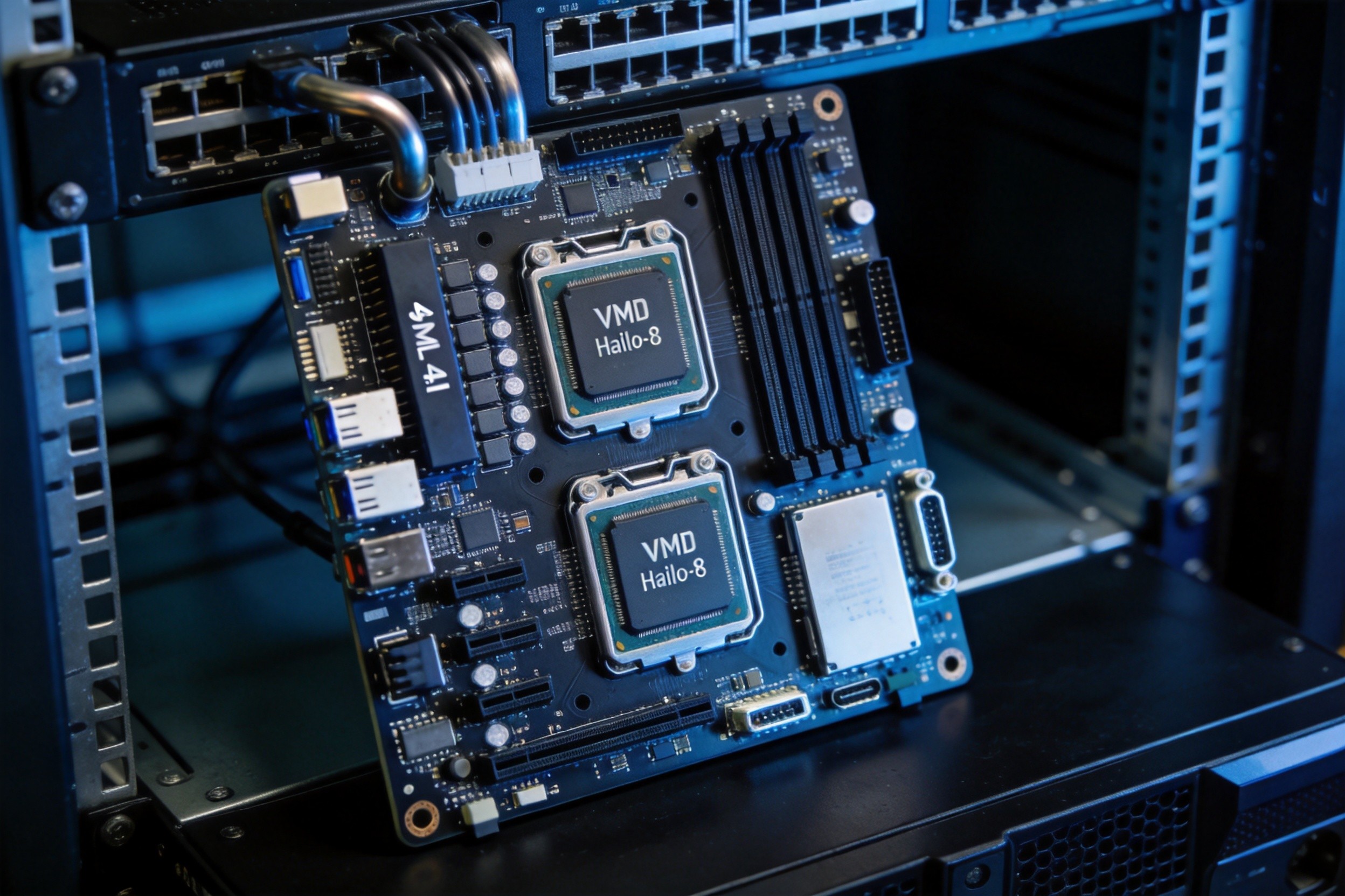
PCB Design Approach: 12-layer board with dual SoC architecture—one for recording management (Intel Atom x7000 series) and one for AI inference (Hailo-8 accelerator via PCIe). 16 GB DDR4 memory (dual-channel, 3200 MHz) for the recording SoC, with 4 GB LPDDR4X dedicated to the Hailo-8. Storage: 4 × SATA III ports for HDD arrays (up to 80 TB raw) plus 1 × NVMe M.2 for AI model cache and metadata indexing. The SATA and PCIe interfaces are routed with impedance-controlled differential pairs on inner layers adjacent to solid ground planes. Thermal design: dual redundant fans with NTC monitoring, 2 oz copper power/ground layers for heat spreading, and thermal vias under both SoCs.
Result: Sustained write throughput of 1.6 Gbps (64 × 1080p/30fps at 4 Mbps per stream), AI-powered person search across 30 days of footage in under 5 seconds, and MTBF exceeding 100,000 hours with dual-fan redundancy.
Future Development Trends
In-Sensor AI and Neuromorphic Vision
Bio-inspired vision sensors that process temporal information directly at the pixel level—rather than capturing full frames for external processing—represent the next frontier in surveillance efficiency. Research-grade MoS2 phototransistor arrays (Nature Nanotechnology, 2024) have demonstrated 99.2% action recognition accuracy with 98% less data than conventional frame-based sensors, by encoding spatiotemporal information at the sensory terminal. Event-driven cameras (e.g., Prophesee Metavision) are already commercially available, generating data only when pixel-level brightness changes occur, dramatically reducing bandwidth and processing requirements. PCB integration of these sensors requires new interface architectures (event-driven rather than frame-based) and co-optimized neural network models. Timeframe: Event-driven cameras are in production for industrial applications; in-sensor AI will enter mainstream surveillance by 2028–2029.
Privacy-Preserving AI and On-Device Anonymization
Growing regulatory pressure (GDPR, China’s Personal Information Protection Law) is driving the development of on-device privacy features that anonymize video at the edge—blurring faces, removing personally identifiable information, and generating only metadata (e.g., “person detected at coordinates X,Y” rather than raw video) for cloud transmission. This requires additional AI processing at the camera level, increasing NPU utilization and thermal load on the PCB. Timeframe: Privacy-preserving AI features are available in premium cameras (2025–2026); regulatory mandates will drive universal adoption by 2028–2030.
5G-Connected Surveillance and Cloud-Edge Architecture
5G connectivity is enabling surveillance cameras in locations where wired Ethernet is impractical (remote infrastructure, temporary installations, mobile surveillance). 5G NR modules (Sub-6 and mmWave) on the camera PCB require RF design expertise—antenna integration, impedance matching, and thermal management for the 5G modem’s power dissipation. The cloud-edge architecture distributes AI workloads: real-time alerts are generated at the edge, while forensic analysis and model training occur in the cloud. Timeframe: 5G cameras are in early deployment; volume production for smart city applications expected by 2027–2028.
Conclusion
Security and surveillance PCB design has evolved from simple video encoding to integrated AI edge computing—where the PCB must simultaneously manage high-speed image sensor interfaces, neural network inference, hardware-accelerated video encoding, encrypted network communication, and cybersecurity hardware roots of trust. The RK3588 and Jetson Orin platforms represent the current state of the art, enabling real-time multi-channel AI analytics at the edge. As the industry moves toward in-sensor AI, privacy-preserving processing, and 5G connectivity, the PCB designer’s role is expanding from digital system layout to heterogeneous computing architecture—integrating vision processing, AI inference, RF communication, and security on a single board that must operate reliably in outdoor environments for years without maintenance. For electronics manufacturers in the surveillance space, the ability to deliver PCBs that balance AI performance, thermal management, and cybersecurity compliance is the key to winning in a market where intelligence is the new baseline.
Need surveillance-grade PCB manufacturing with AI SoC integration support? Connect with our engineering team to discuss edge computing layout strategies, PoE power design, and hardware security implementation.
 English
  简体中文
简体中文  Español
  العربية