
Introduction / Industry Overview
The smart home industry is experiencing a protocol convergence that is fundamentally reshaping PCB design. After years of fragmentation—Zigbee devices that couldn’t talk to Wi-Fi hubs, Bluetooth sensors orphaned by platform changes, and proprietary ecosystems that locked consumers into single-vendor solutions—the Matter protocol (developed by the Connectivity Standards Alliance) is establishing a universal application layer that runs over Thread or Wi-Fi, enabling cross-platform interoperability among Apple Home, Google Home, Amazon Alexa, and Samsung SmartThings.
The global smart home market was valued at approximately USD 101 billion in 2025, projected to reach USD 195 billion by 2030 at a CAGR of 14.2% (Mordor Intelligence, 2025). This growth is driving PCB design toward three imperatives: multi-protocol wireless integration (a single device may need Wi-Fi, BLE, Thread, and Zigbee), ultra-low power consumption (battery-powered sensors must operate for 3–5+ years), and edge AI capability (local voice recognition, presence detection, and anomaly processing without cloud dependency).
This article examines the core technologies, application cases, and future trajectory of smart home PCB design, with emphasis on Matter/Thread protocol integration, multi-protocol RF coexistence, and the power management strategies that enable long battery life.
Core Technology Analysis
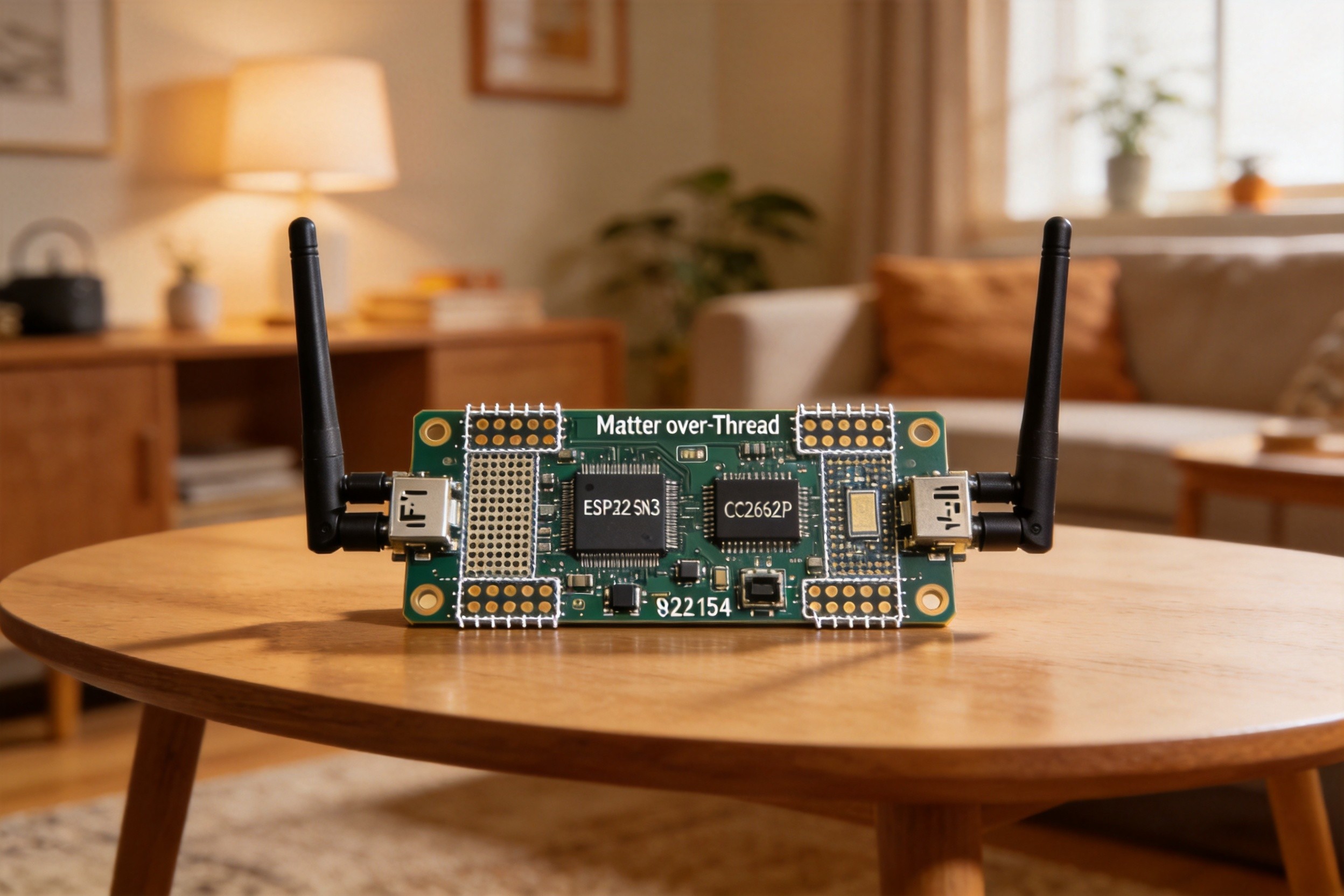
Matter Protocol: PCB Design Impact of the Application Layer
A common misconception is that Matter reduces RF complexity on the PCB. In reality, Matter is a software and application layer—it does not define a radio. It sits above IP and relies on existing transports: primarily Thread (IEEE 802.15.4 at 2.4 GHz) for low-power devices and Wi-Fi (2.4/5/6 GHz) for high-bandwidth devices. The Matter stack, with its security framework (secure boot, device attestation, encrypted group communication), OTA update mechanisms, and multi-admin capability, is memory-intensive—often requiring 512 KB+ flash and 64 KB+ RAM beyond what the base wireless protocol demands.
PCB Design Impact:
| Factor | Zigbee Only | Matter over Thread | Matter over Wi-Fi |
|---|---|---|---|
| MCU Flash Requirement | 128–256 KB | 512–1024 KB | 512 KB+ |
| MCU RAM Requirement | 16–32 KB | 64–128 KB | 128 KB+ |
| RF Complexity | Medium (single 2.4 GHz) | Medium (single 2.4 GHz, same radio as Zigbee) | High (2.4/5 GHz, multi-band) |
| Power Consumption | Lowest | Low–Medium | Highest |
| BOM Cost at Scale | Bajo | Medium | Medium–High |
| Certification Risk | Medium | High (Matter + Thread) | High (Matter + Wi-Fi) |
This means a device that previously used a simple Zigbee SoC (e.g., Silicon Labs EFR32MG21, 768 KB flash, 64 KB RAM) may now need a higher-end Matter-capable SoC (e.g., Silicon Labs MGM240L, 1536 KB flash, 256 KB RAM) even though the underlying radio is the same IEEE 802.15.4 transceiver. The PCB layout is similar, but the BOM cost increases, and the firmware complexity grows substantially.
Multi-Protocol Gateway Design: The most complex smart home PCB is the multi-protocol gateway/hub, which must simultaneously support Wi-Fi (for cloud connectivity and high-bandwidth devices), Thread/Matter (for low-power sensors and actuators), Zigbee (for legacy device compatibility), and BLE (for phone pairing and proximity triggers). The Texas Instruments CC2652P/P7 module exemplifies this challenge, running Matter, Thread, and BLE concurrently through a dual-core architecture—one core for the 802.15.4 MAC layer (Thread/Zigbee) and another for BLE GATT services and Matter application logic. On the PCB, the three RF protocols share the 2.4 GHz band, requiring:
- Antenna diversity: Separate antennas for Wi-Fi and 802.15.4/BLE, positioned at opposite edges of the PCB with ≥20 dB spatial isolation
- Coexistence signaling: Hardware handshake lines between Wi-Fi and BLE/802.15.4 radios that coordinate transmit/receive timing to avoid simultaneous operation
- Power supply isolation: Separate LDO regulators for each RF section, preventing power rail noise from one protocol coupling into another’s sensitive receiver
Wireless Module Selection: Design Decision Framework
The choice of wireless module is a hardware decision with irreversible consequences for BOM cost, PCB complexity, certification timeline, and power consumption. The decision framework starts with the power source:
Mains-powered devices (smart plugs, light switches, cameras): Wi-Fi + BLE is the straightforward choice. ESP32-S3 ($8–15 per module) provides Wi-Fi 6 + BLE 5.0 with direct cloud connectivity, eliminating the need for a separate hub. The PCB is relatively simple (4-layer FR-4, single RF section) but must manage Wi-Fi’s high peak current (300–500 mA) and thermal dissipation (~1W active).
Battery-powered sensors (door/window sensors, motion detectors, temperature/humidity): Zigbee or Thread is mandatory for 3+ year battery life. Wi-Fi’s protocol overhead (association, authentication, DHCP) and high active current make it incompatible with coin-cell or small Li-ion power budgets. The PCB uses a Zigbee/Thread SoC (Silicon Labs EFR32MG24, ~10 mA active, ~1 μA sleep) with a CR2032 or CR2450 battery. The PCB must minimize parasitic leakage currents—every μA of quiescent current reduces battery life by approximately 2 months on a CR2032 (225 mAh capacity).
Security-critical devices (smart locks, alarm panels): Z-Wave’s S2 security framework and mandatory alliance certification provide the strongest interoperability guarantees. The PCB integrates a Z-Wave module (Silicon Labs ZGM230S, 868/908 MHz sub-GHz) with a sub-GHz antenna that provides superior wall penetration compared to 2.4 GHz. However, Z-Wave’s regional frequency differences (868 MHz in Europe, 908 MHz in North America, 921 MHz in ANZ) require region-specific antenna tuning and certification—complicating global product deployment.
Antenna Design Considerations: The most common PCB-level mistake is treating the antenna as an afterthought. A chip antenna placed in the board center with surrounding copper will achieve 5–10 m range instead of the specified 50+ m. Best practices include:
- Position the antenna at the PCB edge with a ground-plane clearance zone per the manufacturer’s reference design
- For 2.4 GHz chip antennas, the ground plane must extend at least λ/4 (~31 mm) from the antenna feed point
- Validate antenna performance in the final production enclosure—plastic housings, metal shielding cans, and nearby batteries can de-tune the antenna by 5–15%, reducing range by 30–50%
- Allocate time for re-tuning the matching network after initial enclosure assembly
Low-Power Design: Achieving 5+ Year Battery Life
For battery-powered smart home devices, power consumption is the primary design constraint. A CR2450 battery (620 mAh) must last 5 years—meaning an average current budget of only 14.2 μA. This budget must cover the MCU, sensor, RF transceiver, and any always-on monitoring circuits.
Design Strategies:
-
Aggressive sleep modes: The MCU spends >99.9% of its time in deep sleep (sub-μA). BLE 5.4 advertising intervals of 1–4 seconds, with connection events only when data needs transmission. Thread end devices use “sleepy” mode, polling their parent router every 5–60 seconds.
-
Wake-on-event architecture: Interrupt-driven design where sensors (PIR motion, reed switch, capacitive touch) wake the MCU only when an event occurs. A door sensor that wakes once per hour for a status report and once per door open/close event draws an average of 2–3 μA, yielding 8+ years on a CR2032.
-
Power gating: Unused peripherals (I2C sensors, LED indicators, debug interfaces) are powered through MOSFET switches that disconnect them from the supply during sleep. A single I2C temperature sensor drawing 1 μA in standby can consume 9 mAh per year—significant when the total budget is 124 mAh/year (CR2032 over 5 years).
-
Efficient voltage regulation: Buck converters for high-current active modes (RF transmission), bypassed by LDOs during sleep to eliminate switching losses. Some modern SoCs integrate DC-DC converters that operate in both buck and bypass modes based on load.
-
Battery life calculation: For a device that wakes every 60 seconds, transmits for 5 ms at 10 mA, and sleeps at 1 μA: average current = (5 ms × 10 mA + 59995 ms × 1 μA) / 60000 ms = 1.83 μA. On a CR2450 (620 mAh), this yields 38.800 hours = 4.4 years—comfortably within the 3–5 year target.
Edge AI Integration: Local Intelligence Without Cloud Dependency
The integration of AI at the device level—local voice recognition for smart speakers, presence detection for lighting, anomaly detection for security—requires adding NPU capabilities to PCBs that were previously simple wireless sensor nodes.
SoC Platforms for Smart Home AI:
- ESP32-S3: Dual-core Xtensa LX7, vector instructions for AI acceleration, 512 KB SRAM. Sufficient for keyword spotting (2–3 wake words) and simple image classification. ~0.5W active.
- Nordic nRF54L15: Cortex-M33 + RISC-V co-processor, 1.5 MB NVM + 256 KB RAM, supports BLE 6.0, Thread, Matter. Edge AI via the RISC-V co-processor running lightweight models.
- Telink TL721X: First BLE Core 6.0 certified multi-protocol SoC, integrates TL-EdgeAI platform for edge AI inference. Sub-mA active current with AI co-processing.
For the PCB, edge AI integration increases memory requirements (external flash for model storage), thermal considerations (sustained AI inference draws 50–100 mA for seconds), and power management complexity (AI inference bursts must not drain the battery or interfere with RF transmission).
Typical Application Cases
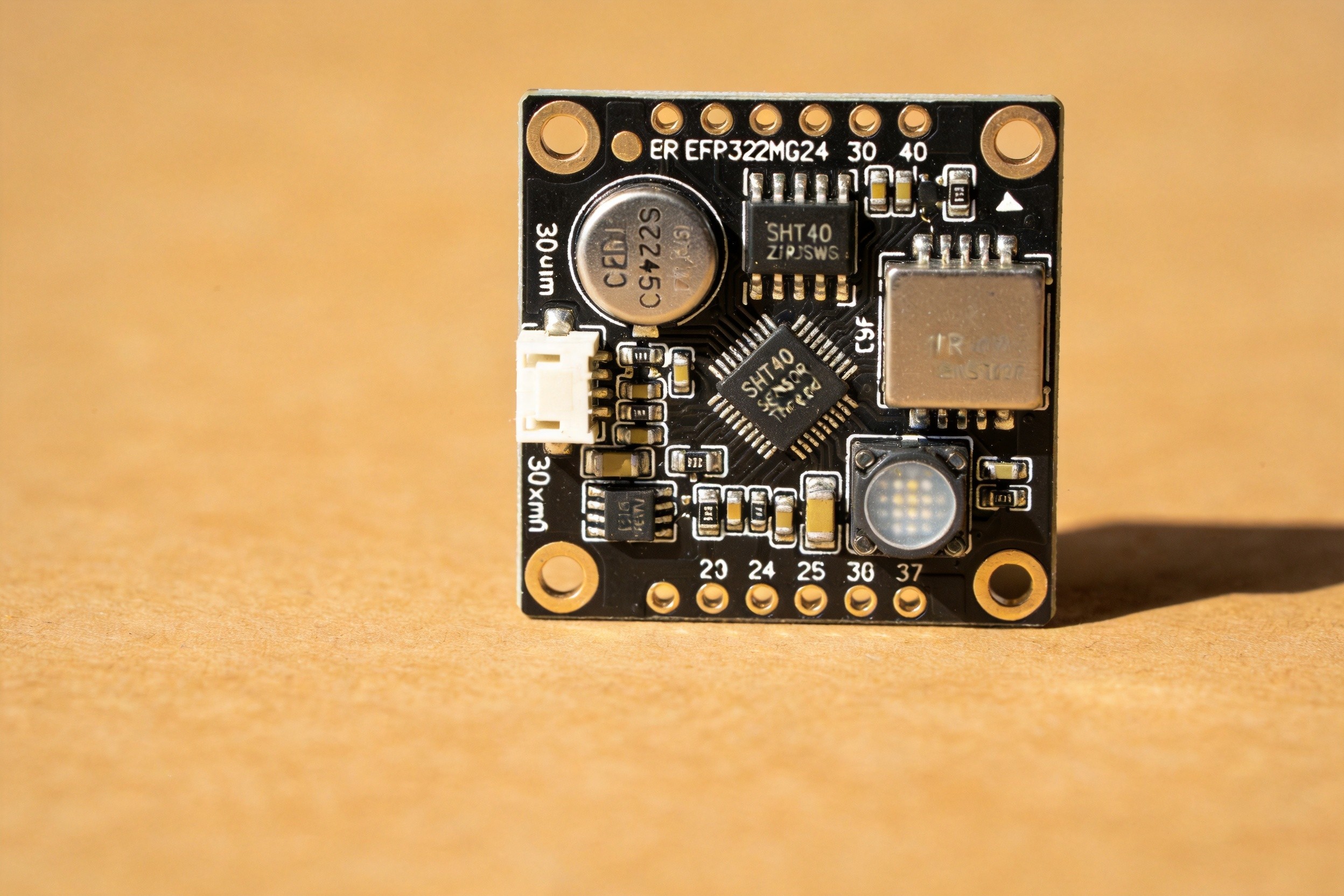
Case 1: Matter-over-Thread Smart Light Switch
A single-gang smart light switch must operate from mains power (120/240 VAC), support Matter over Thread, and maintain responsive local control even when the home network is down.
PCB Design Approach: 4-layer FR-4 with a Silicon Labs MGM240L Matter-over-Thread SoC (1536 KB flash, 256 KB RAM, IEEE 802.15.4 + BLE). Power supply: non-isolated buck converter (120/240 VAC to 3.3V, <50 mW no-load for Energy Star compliance). The relay (16A/250VAC rated) is controlled through an optocoupler for safety isolation. The Thread antenna is a meandering inverted-F antenna (MIFA) etched on the top layer at the PCB edge, with ground clearance per Silicon Labs AN928. A physical button provides local override capability, connected to a GPIO interrupt that wakes the MCU from sleep and toggles the relay regardless of network status. The secure element (ATECC608B) stores the Matter device certificate for commissioning.
Result: Thread range of 35 m through two interior walls, relay switching time <50 ms from button press, Matter commissioning in under 15 seconds via QR code scan, and no-load power consumption of 0.3W (meeting Energy Star requirements).
Case 2: Battery-Powered Multi-Sensor (Temperature, Humidity, Motion, Light)
A coin-cell-powered multi-sensor must operate for 3+ years on a single CR2450, reporting temperature (±0.3°C), humidity (±2% RH), motion (PIR), and ambient light level via Zigbee or Thread.
PCB Design Approach: 4-layer HDI (30 mm × 30 mm) with an EFR32MG24 Zigbee/Thread SoC (768 KB flash, 64 KB RAM). Sensors: Sensirion SHT40 (temperature/humidity, 0.4 μW average power at 1 measurement/minute), AM312 PIR (1 μA standby, interrupt-driven wake), and VEML7700 ambient light sensor (0.5 μA standby). The PCB uses a ground-plane-integrated inverted-F antenna optimized for the device’s plastic enclosure (tuned empirically with a VNA after enclosure integration). Power gating disconnects all sensors between measurement cycles. The device wakes every 60 seconds for environmental readings and immediately on PIR trigger, transmitting a 20-byte payload in <3 ms at 0 dBm.
Result: Average current consumption of 3.2 μA, yielding 620 mAh / 3.2 μA = 193,750 hours = 22.1 years theoretical (practical life limited by battery self-discharge to 5–7 years). Zigbee range of 20 m through one interior wall, with 99.5% message delivery rate in a typical home environment.
Case 3: Smart Home Gateway — Multi-Protocol Hub
A smart home gateway must bridge Matter-over-Thread, Zigbee 3.0, BLE, and Wi-Fi 6, supporting up to 200 connected devices with sub-second response time for local automations.
PCB Design Approach: 6-layer HDI with an ESP32-S3 (Wi-Fi 6 + BLE) as the main processor, a CC2652P (Thread + Zigbee), and an OpenThread border router stack. The ESP32-S3 handles Wi-Fi connectivity, cloud communication, and the main application logic. The CC2652P manages Thread and Zigbee networks, communicating with the ESP32-S3 via UART at 1 Mbps. The two RF sections use separate chip antennas positioned at opposite ends of the 80 mm × 80 mm PCB, with a grounded via fence between them providing >25 dB isolation. Ethernet connectivity (RJ45 with integrated magnetics, IEEE 802.3at PoE input) provides a wired backhaul option. The gateway runs Home Assistant or a similar open-source platform, with Matter controller functionality enabling direct commissioning of Thread and Wi-Fi devices.
Result: Thread/Zigbee mesh network supporting 200+ devices, Wi-Fi throughput of 500 Mbps (Wi-Fi 6), local automation latency of <200 ms (sensor event to actuator response), and PoE power consumption of 5.2W.
Future Development Trends
Matter 1.4+ and Expanded Device Categories
The Matter specification is rapidly expanding beyond lighting and sensors to include energy management (EV chargers, solar inverters, smart thermostats), security cameras (Matter camera device type expected in Matter 1.5), robotic vacuums, and major appliances. Each new device type brings specific PCB requirements—higher power delivery for EV chargers, high-speed interfaces for cameras, motor control for appliances—while maintaining Matter compatibility and security certification. Timeframe: Energy management devices are specified in Matter 1.4 (2026); cameras and appliances expected in Matter 1.5–1.6 (2027–2028).
Thread Border Router Integration in Wi-Fi Access Points
Thread border router functionality is being integrated directly into consumer Wi-Fi routers (Apple HomePod Mini, Google Nest Hub, Eero 6+), eliminating the need for a separate hub device for Thread networks. For PCB designers at networking equipment companies, this means adding an 802.15.4 radio co-processor and antenna alongside the existing Wi-Fi RF section, with coexistence management between the two 2.4 GHz radios. Timeframe: Already shipping in premium routers; mainstream adoption by 2027.
Energy Harvesting for Perpetual Smart Home Sensors
The convergence of ultra-low-power design with energy harvesting (solar, thermal, RF) is approaching the threshold for “perpetual” sensors that never need battery replacement. Indoor solar cells can generate 10–50 μW from ambient lighting—sufficient to power a Thread end device that wakes once per minute. The PCB must integrate a solar cell, an energy management IC (e.g., e-peas AEM3094 with MPPT), and a supercapacitor or rechargeable battery for energy buffering. Timeframe: Prototype perpetual sensors are demonstrated (2025–2026); commercial products will emerge by 2028–2029 as energy harvesting efficiency improves.
Conclusion
Smart home PCB design is being reshaped by the Matter protocol’s promise of universal interoperability—but Matter does not simplify the PCB; it shifts complexity from the RF layer to the MCU and firmware layer, demanding higher-end processors and larger memory footprints even when the underlying radio technology remains unchanged. Multi-protocol gateways represent the most complex PCBs in the smart home space, requiring simultaneous management of Wi-Fi, Thread/Zigbee, and BLE with coexistence signaling and antenna diversity. For battery-powered devices, the sub-μA sleep current imperative drives every design decision from component selection to PCB leakage current management. As the industry moves toward edge AI integration, Thread border router consolidation in Wi-Fi access points, and energy harvesting for perpetual sensors, the PCB designer’s challenge is expanding from wireless connectivity to intelligent, autonomous, and self-sustaining edge computing. For electronics manufacturers targeting the smart home market, the ability to deliver PCBs that balance multi-protocol RF performance, ultra-low power, and Matter certification compliance is the prerequisite for ecosystem participation.
Need smart home PCB manufacturing with Matter certification support? Connect with our team to discuss multi-protocol RF layout, antenna optimization, and low-power design strategies for connected home devices.
 English
  简体中文
简体中文  Español
  العربية