
Introduction / Industry Overview
Audio equipment sits at the intersection of art and engineering, where the fidelity of an electrical signal determines whether a listener experiences a performance as the artist intended. The global professional audio equipment market was valued at approximately USD 12.8 billion in 2024, with a projected compound annual growth rate (CAGR) of 7.2% through 2030, driven by the expansion of content creation, live event production, and immersive audio formats (Frost & Sullivan, 2024). Within the broader electronic manufacturing landscape, audio PCBs occupy a specialized niche: they are not the highest-volume segment, but they demand some of the most rigorous signal integrity standards in the industry.
The fundamental challenge is deceptively simple—preserve a 20 Hz to 20 kHz analog waveform from input to output without adding noise, distortion, or coloration. In practice, this means managing microvolt-level signals alongside high-current power stages on the same board, while keeping crosstalk below −90 dB and total harmonic distortion plus noise (THD+N) under 0.005% in professional-grade equipment. The PCB is not merely a substrate; it is an active participant in the signal chain, and every layout decision has an audible consequence.
This article examines the core technologies, application cases, and future trends shaping audio equipment PCB design, with particular emphasis on signal integrity, converter architectures, and the standards that define acceptable performance.
Core Technology Analysis
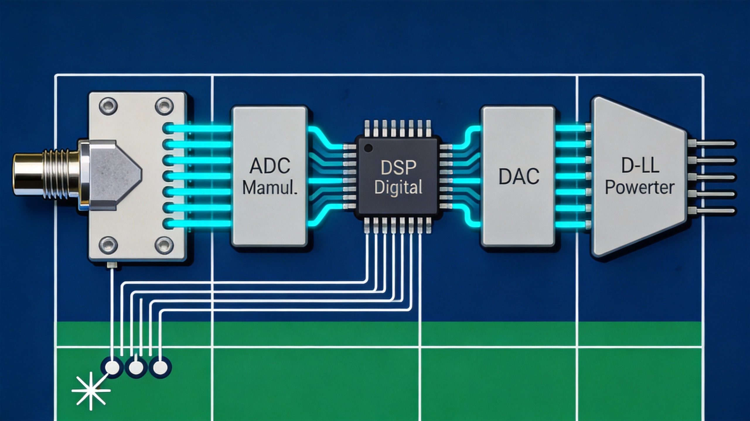
Audio Signal Chain and PCB Layout Fundamentals
The audio signal chain—from transducer input through preamplification, analog-to-digital conversion (ADC), digital signal processing (DSP), digital-to-analog conversion (DAC), and power amplification—imposes distinct PCB design requirements at each stage. The single most critical principle is physical segregation of functional domains.
A well-designed audio PCB divides the board into four zones: analog front-end (microphone preamps, input buffers), digital processing (DSP, MCU, clock circuits), power management (regulators, filtering), and power output (amplifier output stages). These zones must maintain sufficient spacing to prevent electromagnetic coupling, and in many designs, isolation slots (routed gaps in the copper) or metal shield cans are employed to create physical barriers between sensitive analog circuits and noisy digital or switching sections.
Grounding strategy is paramount. Star grounding—where all ground returns converge at a single reference point near the power supply input—remains the gold standard for analog audio. Each functional zone has its own ground plane, and these planes connect only at the star point, typically through a 0-ohm resistor or ferrite bead. This topology eliminates ground loops, the primary cause of 50/60 Hz hum in audio systems. For mixed-signal designs, the analog and digital ground planes are split and joined at a single controlled juncture beneath the ADC or DAC, ensuring that digital switching currents do not flow through the analog return path.
High-Performance DAC/ADC Architectures and PCB Implications
The DAC is the gatekeeper of audio quality in the digital-to-analog transition. Two architectures dominate modern audio equipment:
Delta-Sigma (ΔΣ) DACs are the prevailing choice for high-fidelity applications. They employ oversampling and noise-shaping to push quantization noise out of the audible band, achieving resolutions of 24 bits and beyond with THD+N figures below 0.0004% in flagship devices like the ESS ES9038PRO. The PCB design challenge for ΔΣ DACs centers on clock integrity—the jitter on the master clock directly modulates the noise floor. Clock traces must be routed as short, impedance-controlled lines with continuous ground-plane referencing, and the crystal oscillator or PLL should be placed immediately adjacent to the DAC with dedicated power filtering.
R-2R Ladder DACs remain favored by a segment of the audiophile community for their perceived natural timbre. They require precisely matched resistor networks, and any thermal gradient across the R-2R network introduces linearity errors. PCB layout must ensure symmetric thermal distribution around the DAC, avoiding placing heat-generating components (such as voltage regulators) asymmetrically near the resistor array.
On the ADC side, the industry is witnessing a paradigm shift from voltage-mode instrumentation amplifiers to current-conveyor-based analog front ends (AFEs). The Triad Semiconductor TS5510 exemplifies this transition, achieving a 156 dB Total Input Capture Range (TICR) spanning from −128 dBu to +28 dBu. This architecture eliminates the need for external resistive pads—traditionally required to prevent clipping on loud sources—which degrade the noise floor. On the PCB, current-conveyor AFEs demand careful attention to the input trace impedance and the reference ground quality, as the high-impedance input nodes are extremely susceptible to capacitive coupling from adjacent traces.
EMI/EMC Compliance and the IEC 60268 Standard Framework
Audio equipment must satisfy both emission and immunity requirements under EMC regulations (FCC Part 15, EN 55032), and the functional performance of the audio path is evaluated under the IEC 60268 family of standards.
IEC 60268 comprises 21+ parts covering the full range of sound system equipment. Key sections relevant to PCB design include:
- IEC 60268-3 (Amplifiers): Specifies methods for measuring frequency response, THD, and signal-to-noise ratio. Professional-grade amplifiers must achieve THD below 0.5% at rated output.
- IEC 60268-4 (Microphones): Defines sensitivity, directional response, and dynamic range measurements. PCB noise in microphone preamplifiers must remain below the thermal noise floor of the transducer.
- IEC 60268-7:2025 (Headphones and earphones): The latest fourth edition, published in June 2025, introduces updated measurement methods for modulation distortion, difference-frequency distortion, and left-right tracking response for stereo headphones. PCB designers for headphone amplifiers must ensure channel matching to within 0.5 dB to meet the new tracking specifications.
- IEC 60268-16 (Speech intelligibility): Requires networked audio devices to achieve 99.99% packet integrity and clock synchronization better than 1 μs—parameters that directly constrain the jitter budget on digital audio PCBs.
For EMI suppression, the PCB designer’s toolkit includes multi-stage power supply filtering (LC filters with low-ESR capacitors placed within 1–2 mm of IC power pins), guard traces around sensitive analog inputs (ground-stitched copper pours flanking high-impedance nodes), and controlled-impedance differential routing for balanced audio interfaces (XLR, AES/EBU) targeting 100-ohm differential impedance with ±5% tolerance.
Class-D Amplifier PCB Design: Efficiency Meets Complexity
Class-D amplifiers have become the dominant topology in both consumer and professional audio, achieving efficiencies above 90% through pulse-width modulation (PWM). However, the high-frequency switching (typically 300–800 kHz) generates broadband EMI that can couple into sensitive analog circuits if the PCB layout is not meticulously managed.
Key PCB design rules for Class-D amplifiers:
- Gate drive loops must be minimized. The loop formed by the gate driver output, the MOSFET gate, and the return path must be kept under 5 mm in total length to reduce parasitic inductance, which causes ringing and increased switching losses.
- Output filter placement. The LC reconstruction filter must be placed as close to the amplifier output as possible, with the inductor and capacitor ground returns connected directly to the star ground point.
- Split power planes. Separate the PWM power stage’s ground plane from the analog front-end’s ground plane, connecting them only at the star point, to prevent high-di/dt switching currents from modulating the analog reference.
The emergence of GaN (gallium nitride) power transistors in Class-D output stages is enabling switching frequencies above 2 MHz, which shrinks the output filter size and extends the amplifier’s bandwidth. GaN devices, however, have even faster dv/dt transitions, making PCB parasitic management even more critical—the gate drive loop must be treated as an RF design problem with via stitching, coplanar waveguide structures, and electromagnetic simulation.
Typical Application Cases
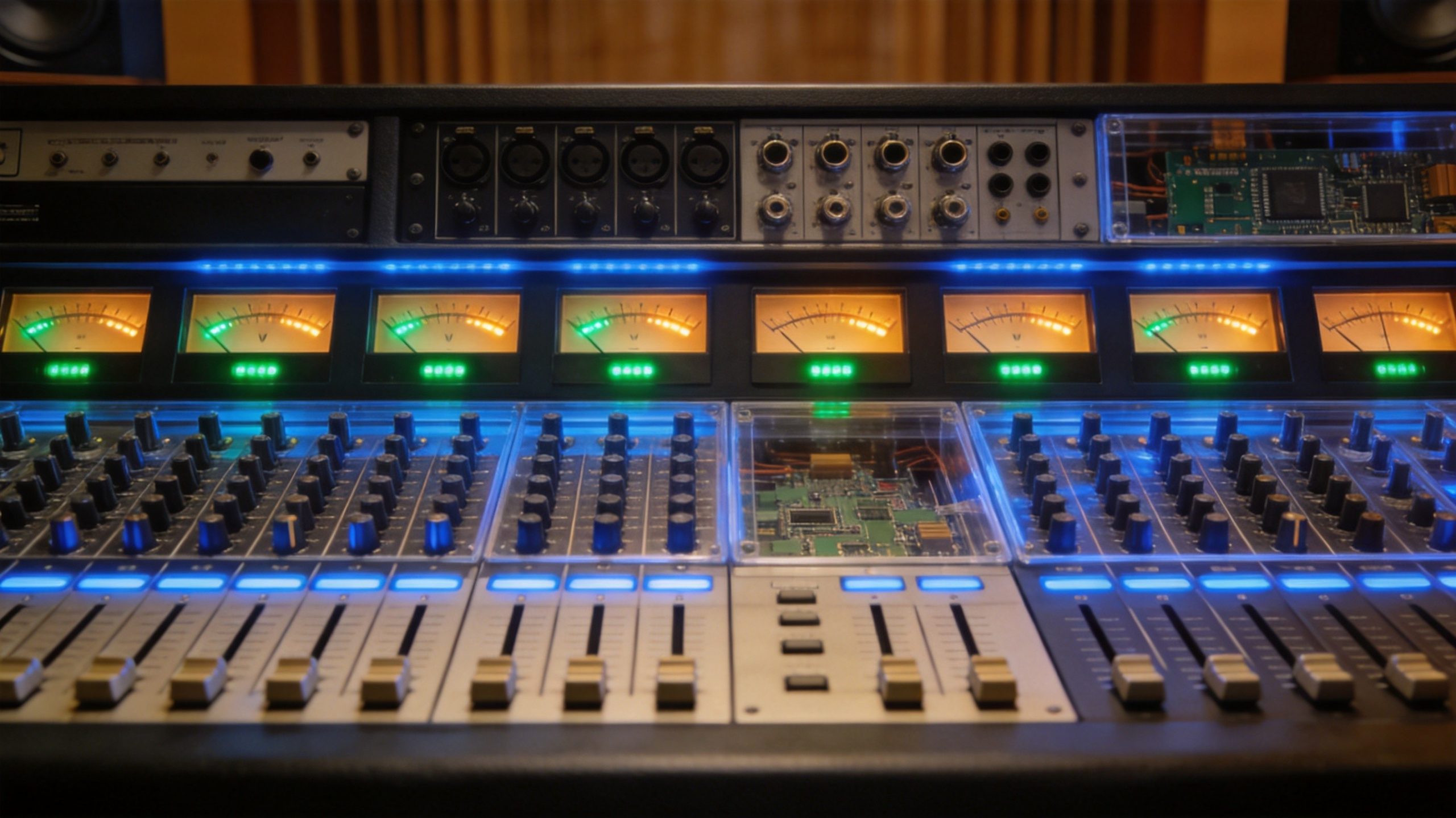
Case 1: Professional Studio Recording Console — Analog Front End Design
A professional recording console must capture signals ranging from a whisper at −60 dBu to a kick drum at +20 dBu without gain staging adjustments. The traditional solution uses a voltage-mode instrumentation amplifier with switchable pads, but pad engagement degrades the noise floor by 10–20 dB.
Solution: A current-conveyor AFE (such as the TS5510) with 156 dB TICR eliminates the external pad entirely. The PCB layout places the AFE as close to the XLR input connector as possible—within 10 mm—to minimize trace length picking up EMI. The input traces are routed as differential pairs with ground-guard traces, and the AFE’s SPI-controlled gain adjustment is handled by a dedicated microcontroller section located on the opposite side of the board with a ground-plane shield between them.
Result: THD+N of 0.003% across the full input range, SNR exceeding 120 dB, and zero gain-staging adjustments required during a recording session. The console achieves a speech transmission index (STI) above 0.65 per IEC 60268-16, even in high-RF environments near broadcast transmitters.
Case 2: Networked PA System — Dante Audio Over Ethernet
A large-venue public address system uses Dante (Audio over IP) to distribute 64 channels of 48 kHz/24-bit audio across standard Ethernet infrastructure. The PCB integrates a Dante interface module, a DSP engine, and multiple DAC channels on a single board.
Challenge: The Dante module’s Ethernet PHY generates significant switching noise at 125 MHz (for Gigabit Ethernet) that can couple into the DAC analog outputs if not properly isolated.
Solution: A split-plane architecture with the Ethernet PHY and magnetics on one side of the board and the DAC/analog section on the other, separated by a ground-stitched isolation slot. Power for the Dante module is supplied through a dedicated isolated DC-DC converter, and the DAC’s voltage reference is derived from a separate low-noise LDO with its own ground reference. Differential clock distribution from a master clock IC ensures jitter below 50 ps at the DAC clock input, measured using a phase-noise analyzer.
Result: End-to-end latency of 1.0 ms (2 samples at 48 kHz), packet loss rate below 10⁻⁸, and analog output noise floor of −110 dBu—well within the IEC 60268-16 requirement for professional networked audio.
Case 3: Hi-Fi Class-D Amplifier with GaN Output Stage
A high-end consumer amplifier uses GaN FETs in a Class-D output stage, switching at 1.5 MHz to achieve a −3 dB bandwidth of 80 kHz and THD+N below 0.005% at 100 W into 8 ohms.
PCB Design Approach: The output stage uses a four-layer PCB with a dedicated ground plane on layer 2 directly beneath the gate drive traces on layer 1. The GaN FETs are placed in a half-bridge configuration with less than 3 mm between the high-side and low-side devices to minimize the parasitic inductance of the switching node. Thermal vias (0.3 mm diameter, 0.5 mm pitch) under each FET’s drain pad conduct heat to a copper pour on the bottom layer, which is attached to an external heatsink via a thermal interface material. The output LC filter uses a low-DCR air-core inductor and a polypropylene film capacitor, both surface-mounted within 5 mm of the switching node.
Result: Measured efficiency of 93% at full load, EMI compliance with EN 55032 Class B with 6 dB margin, and thermal rise of only 25°C above ambient at full power—eliminating the need for a cooling fan.
Future Development Trends
32-Bit Float Recording and the End of Gain Staging
The adoption of 32-bit floating-point recording in field recorders and DAWs promises to eliminate the risk of digital clipping entirely—the format’s dynamic range exceeds 1500 dB. However, this promise is only realized if the analog front end can capture the full acoustic dynamic range without saturation. Current-conveyor AFEs with 150+ dB TICR are the first analog architectures capable of matching the capture potential of 32-bit float, enabling “set and forget” gain levels where the engineer no longer needs to adjust gain during a session. Timeframe: This capability is already available in premium products (2025–2026) and will cascade to mid-range equipment by 2028–2029.
GaN-Enabled Class-D Amplification and Software-Defined Audio
GaN power transistors are driving Class-D switching frequencies into the multi-MHz range, enabling output filters small enough for compact modules while maintaining audiophile-grade bandwidth and distortion performance. Combined with DSP-based room correction and active crossover, this trend is converging toward Software-Defined Audio (SDA), where the amplifier’s frequency response, crossover points, and even its “analog character” are defined by firmware rather than passive components. The PCB implications are significant: SDA amplifiers require high-speed data interconnects (SPI, I²S) alongside high-power switching stages, demanding rigorous signal integrity simulation and mixed-signal layout expertise. Timeframe: GaN Class-D is already in production; SDA architectures will become mainstream in professional and premium consumer products by 2027–2028.
Immersive and Spatial Audio Standards (IEC 60268-23)
The upcoming IEC 60268-23 standard will establish the first formal test methodology for three-dimensional sound field reconstruction, including height-channel separation and object-based audio localization accuracy. This standard directly impacts PCB design for immersive audio processors (Dolby Atmos, DTS:X, Sony 360 Reality Audio), which must route dozens of synchronized audio channels with sub-microsecond timing alignment. PCB designers will need to adopt clock-tree synthesis techniques borrowed from high-speed digital design, ensuring that latency across all channels is matched to within a few nanoseconds. Timeframe: The standard is in development, with publication expected by 2027; immersive audio PCBs are already shipping in consumer AV receivers and will expand to automotive and VR applications by 2028–2030.
Conclusion
Audio equipment PCB design is a discipline where microvolts matter and every copper trace is a potential antenna for interference. Success demands a rigorous approach to signal chain architecture, grounding topology, component placement, and EMI mitigation—all validated against the quantitative performance criteria defined in the IEC 60268 standard family. As the industry moves toward 32-bit float capture, GaN-based Class-D amplification, and immersive spatial audio, the PCB designer’s role is evolving from circuit-board layout to system-level signal integrity engineering. For electronics manufacturers seeking to compete in the professional and high-fidelity audio market, investing in advanced mixed-signal PCB design capability is not optional—it is the prerequisite for products that meet the ear’s exacting standards.
Ready to discuss your audio equipment PCB project? Contact our engineering team to explore design solutions tailored to your signal integrity requirements.
 English
  简体中文
简体中文  Español
  العربية