Home > Integrated Circuits ICs > ADG1434YRUZ-REEL7

ADG1434YRUZ-REEL7


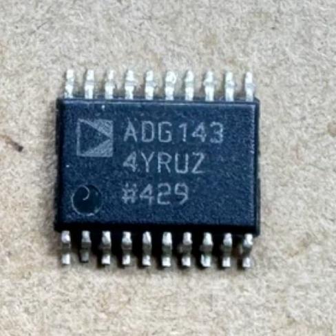
Quad SPDT analog switch, 4Ohm Ron, +/-15V/+12V/+/-5V, 115mA/ch, BBM, -70dB off-isolation, 200MHz BW, TSSOP-20, -40~125C

3000

Effective Inventory
Go to Inquiry

Image for reference only

Manufacturer Part:

ADG1434YRUZ-REEL7

Package:

TSSOP-20 (RU-20) (6.5 x 4.4 x 1.05 mm, 0.65mm pitch)

Brand:
Product Categories:
Other recommendations you may be interested in.
Description

The ADG1434YRUZ-REEL7 from Analog Devices is a quad SPDT (single-pole, double-throw) iCMOS analog switch with 4 Ohm typical on-resistance in a 20-lead TSSOP package with tape and reel packaging (7-inch reel). Key specifications at plus or minus 15 V dual supply: on-resistance 4 Ohm typical (4.7 Ohm maximum at 25 degrees C, 5.7 Ohm maximum at 85 degrees C, 6.7 Ohm maximum at 125 degrees C); on-resistance match between channels 0.55 Ohm typical; on-resistance flatness 0.5 Ohm typical; analog signal range VSS to VDD (rail-to-rail); continuous current per channel up to 115 mA; source off leakage 0.02 nA typical (3 nA max at 85 degrees C); drain off leakage 0.02 nA typical; channel on leakage 0.04 nA typical; transition time 315 ns typical at plus or minus 5 V (170 ns at plus or minus 15 V); break-before-make time delay 90 ns minimum; turn-on time 325 ns typical at plus or minus 5 V; turn-off time 150 ns typical at plus or minus 5 V; charge injection -10 pC typical at plus or minus 5 V; off isolation -70 dB typical at 1 MHz; channel-to-channel crosstalk -70 dB typical at 1 MHz; THD plus N 0.06 percent typical at 20 Hz to 20 kHz; -3 dB bandwidth 145 MHz typical at plus or minus 5 V (200 MHz at plus or minus 15 V); digital inputs 3 V logic compatible (VIH = 2.0 V, VIL = 0.8 V); supply current IDD = 18 uA typical, ISS = 0.5 uA typical; rated for plus or minus 15 V, plus 12 V single, or plus or minus 5 V dual supply operation; operating temperature -40 to +125 degrees C (Y version); EN input on LFCSP version (not on TSSOP); break-before-make switching action; iCMOS process; RoHS compliant. Production status.

The ADG1434YRUZ-REEL7 from Analog Devices is a quad SPDT (4-channel, 2:1 multiplexer) analog switch built on the iCMOS (industrial CMOS) process, offering very low on-resistance (4 Ohm typical) with excellent on-resistance flatness (0.5 Ohm) and channel matching (0.55 Ohm), making it ideal for precision signal routing applications where distortion and signal integrity are critical.

The iCMOS process is Analog Devices’ proprietary technology that combines high-voltage CMOS with bipolar transistors, enabling analog switches that can operate at high supply voltages (up to plus or minus 16.5 V or 33 V single supply) while achieving low on-resistance and low power consumption. Traditional high-voltage CMOS switches have on-resistance values of 50-200 Ohms; the iCMOS process achieves 4 Ohm, a 10-50x improvement.

The ADG1434 contains four independently controlled SPDT switches. Each SPDT switch has one common terminal (D) and two selectable terminals (S1, S2). The control input (INx) selects which terminal is connected to the common: when INx is LOW, S1A is connected to DA; when INx is HIGH, S1B is connected to DA. Each switch operates independently, and the four switches can be used to route four different signals simultaneously.

The 4 Ohm typical on-resistance is one of the lowest available for a plus or minus 15 V analog switch. This low on-resistance minimizes signal attenuation and voltage error when the switch is in the signal path. For example, with a 10 kOhm load, a 4 Ohm switch introduces only 0.04 percent voltage error (4 / 10004), which is negligible for most applications.

The on-resistance flatness of 0.5 Ohm is equally important. On-resistance varies with the analog signal voltage (because the MOSFET gate-source voltage changes as the analog signal swings), and this variation causes distortion. A 0.5 Ohm flatness means the on-resistance varies by only plus or minus 0.25 Ohm over the full analog signal range, resulting in very low distortion (0.06 percent THD+N). This is critical for audio and precision measurement applications.

The break-before-make (BBM) switching action ensures that the currently connected channel is disconnected before the new channel is connected, preventing momentary short circuits between the two signal sources. The BBM time delay is guaranteed to be at least 90 ns, which is sufficient to prevent short-circuit current spikes but short enough to minimize the signal glitch duration.

The very low leakage currents (0.02 nA typical off-leakage at 25 degrees C) ensure that signals on disconnected channels do not bleed through to the output. At 85 degrees C, the maximum off-leakage is only 3 nA, which for a 100 kOhm source impedance produces only 300 uV of crosstalk voltage – well below the noise floor of most measurement systems.

The plus or minus 15 V supply capability makes the ADG1434 suitable for professional audio equipment (which typically uses plus or minus 15 V analog supplies), industrial instrumentation, and data acquisition systems that need to switch signals with up to plus or minus 10 V amplitude. The device can also operate from a single plus 12 V supply (with GND = 0 V and VSS = 0 V) or from plus or minus 5 V supplies for lower-voltage systems.

The 200 MHz -3 dB bandwidth at plus or minus 15 V allows the switch to pass high-frequency signals without significant attenuation. Combined with the low on-resistance, this makes the ADG1434 suitable for video routing and high-speed data acquisition.

The ADG1434 is the quad SPDT version; the ADG1433 is the triple SPDT version with EN input, available in both TSSOP-16 and LFCSP-16. The ADG1434 in TSSOP-20 does not have an EN pin (all channels are always active); the LFCSP-20 version includes an EN pin. For applications requiring the EN function, use ADG1434YCPZ-REEL7 instead.

The -70 dB off-isolation at 1 MHz and -70 dB channel-to-channel crosstalk ensure excellent signal integrity when multiple channels are used simultaneously. These specifications degrade at higher frequencies but remain acceptable for most audio and instrumentation applications up to several MHz.

The ADG1434YRUZ-REEL7 operates as a set of four independently controlled SPDT analog switches using enhancement-mode N-channel and P-channel MOSFETs in a T-switch configuration, fabricated on the iCMOS process.

Switch Element: Each SPDT switch position uses a complementary NMOS/PMOS pair connected in parallel. The NMOS transistor conducts the negative half of the analog signal, while the PMOS transistor conducts the positive half. Together, they provide rail-to-rail signal handling from VSS to VDD. The on-resistance of the NMOS and PMOS transistors varies in opposite directions with the analog signal voltage: as the signal rises toward VDD, the NMOS RDS(on) increases while the PMOS RDS(on) decreases. The parallel combination produces a relatively flat on-resistance characteristic over the signal range, resulting in the 0.5 Ohm flatness specification.

iCMOS Process: The iCMOS (industrial CMOS) process differs from standard CMOS by incorporating high-voltage DMOS (Double-diffused MOS) transistors that can withstand up to 33 V between drain and source. This enables the ADG1434 to operate at plus or minus 15 V supplies while maintaining low on-resistance. In a standard CMOS process, the MOSFET on-resistance increases dramatically with voltage rating due to the longer channel and heavier drift region required. The iCMOS process uses a lateral DMOS structure that separates the high-voltage blocking region from the channel region, achieving both high voltage capability and low on-resistance simultaneously.

Switch Control: Each SPDT switch has a control input (INx). The control logic is non-inverting: when INx is LOW (below 0.8 V), the A-side switch is closed (S1A connected to D1) and the B-side switch is open; when INx is HIGH (above 2.0 V), the B-side switch is closed (S1B connected to D1) and the A-side switch is open. The digital inputs are 3 V logic compatible, meaning they can be driven by 3.3 V logic even when the analog supplies are plus or minus 15 V. The level shifting is done internally.

Break-Before-Make: The BBM circuit ensures a minimum dead time (90 ns) between opening one switch and closing the other. During this dead time, the common terminal (D) is floating (high impedance). The BBM action prevents the two signal sources (S1A and S1B) from being momentarily connected together, which would cause current to flow from the higher voltage source to the lower voltage source, potentially damaging the source or causing signal glitches. The BBM time is controlled by an internal delay circuit.

Charge Injection: When a MOSFET switch transitions from on to off, the gate charge that was inducing the channel must go somewhere, and a small amount (charge injection) is coupled to the analog signal path through the gate-to-channel capacitance. The ADG1434 has a charge injection of -10 pC at plus or minus 5 V. The negative sign indicates that the output voltage steps negative when the switch turns off. At plus or minus 15 V, the charge injection is typically -50 pC. The charge injection is relatively constant over the analog signal range, which means it can be partially compensated by adding an equal and opposite charge injection from a dummy switch driven by the complementary control signal.

Leakage Currents: When a switch is off, the NMOS and PMOS transistors are both in cutoff, and only the subthreshold leakage and junction leakage currents flow. The 0.02 nA typical off-leakage at 25 degrees C is achieved by careful layout and process design to minimize junction areas and surface leakage paths. At 125 degrees C, the leakage increases due to the temperature dependence of the subthreshold current and junction reverse saturation current, but remains below 8 nA.

Bandwidth and Isolation: The -3 dB bandwidth of 145 MHz at plus or minus 5 V is determined by the RC time constant of the on-resistance (4 Ohm) and the off-state capacitance of the switch and PCB trace. The off-isolation (-70 dB at 1 MHz) is determined by the parasitic capacitance between the open switch terminal and the common terminal, which creates a capacitive voltage divider with the load impedance. At higher frequencies, the isolation degrades because the capacitive reactance decreases. The channel-to-channel crosstalk (-70 dB at 1 MHz) is determined by the parasitic capacitance between adjacent switch channels on the die and in the package.

Power Dissipation: The ADG1434 draws very low supply current (IDD = 18 uA, ISS = 0.5 uA typical) for the internal logic and control circuits. The power dissipation is dominated by the load current through the on-resistance: P = I^2 x RON. At 115 mA per channel, the power dissipation per channel is 115^2 x 4 = 53 mW. With all four channels carrying 115 mA, total switch dissipation is 212 mW, plus the quiescent dissipation.

Pin Name Type Description
1 S1A Analog I/O Switch 1, A-side source terminal; when IN1 is LOW, S1A is connected to D1 (switch closed); when IN1 is HIGH, S1A is disconnected (switch open); signal range VSS to VDD; bidirectional; connect to signal source or destination depending on application
2 D1 Analog I/O Switch 1, common (drain) terminal; the signal routing node that connects to either S1A or S1B depending on IN1 state; bidirectional; signal range VSS to VDD; this is typically the output of the multiplexer or the input to the demultiplexer
3 S1B Analog I/O Switch 1, B-side source terminal; when IN1 is HIGH, S1B is connected to D1 (switch closed); when IN1 is LOW, S1B is disconnected (switch open); signal range VSS to VDD; bidirectional
4 S2A Analog I/O Switch 2, A-side source terminal; controlled by IN2; same characteristics as S1A; independent of Switch 1
5 D2 Analog I/O Switch 2, common (drain) terminal; same characteristics as D1; independent of Switch 1
6 S2B Analog I/O Switch 2, B-side source terminal; controlled by IN2; same characteristics as S1B
7 GND Ground Digital ground reference; connect to system ground; the digital control inputs are referenced to GND; GND can be different from VSS (e.g., VSS = -15 V, GND = 0 V); the GND pin must be connected even if all control inputs are driven from 0/5 V logic
8 VSS Power Negative analog supply; -15 V typical for dual supply operation; -4.5 V to -16.5 V; connect to GND (0 V) for single supply operation; must not exceed VDD in voltage; bypass with 0.1 uF ceramic capacitor to GND near the pin
9 IN4 Digital Input Switch 4 control input; 3 V logic compatible; LOW selects A-side (S4A to D4); HIGH selects B-side (S4B to D4); VIH min 2.0 V; VIL max 0.8 V; can be driven by 3.3 V or 5 V logic; input current less than 0.1 uA
10 S4A Analog I/O Switch 4, A-side source terminal; controlled by IN4
11 D4 Analog I/O Switch 4, common (drain) terminal; controlled by IN4
12 S4B Analog I/O Switch 4, B-side source terminal; controlled by IN4
13 S3B Analog I/O Switch 3, B-side source terminal; controlled by IN3
14 D3 Analog I/O Switch 3, common (drain) terminal; controlled by IN3
15 S3A Analog I/O Switch 3, A-side source terminal; controlled by IN3
16 IN3 Digital Input Switch 3 control input; same specifications as IN4
17 IN1 Digital Input Switch 1 control input; same specifications as IN4
18 VDD Power Positive analog supply; +15 V typical for dual supply; +4.5 V to +16.5 V; bypass with 0.1 uF ceramic capacitor to GND near the pin; for single supply operation, VDD is the positive supply and VSS connects to GND
19 IN2 Digital Input Switch 2 control input; same specifications as IN4
20 GND Ground Digital ground reference; connect to system ground; both GND pins (7 and 20) must be connected externally
Application Description
Professional Audio Signal Routing Route audio signals between multiple sources and destinations; 4 Ohm on-resistance and 0.5 Ohm flatness ensure 0.06 percent THD+N for transparent audio switching; plus or minus 15 V supply handles professional audio levels (up to plus or minus 10 V); BBM prevents click/pop during switching; -70 dB off-isolation ensures crosstalk is inaudible; replace mechanical relays with solid-state speed and reliability
Data Acquisition Input Multiplexer Route one of two sensor inputs to each of four ADC channels; 4 Ohm on-resistance with 10 kOhm ADC input impedance causes only 0.04 percent gain error; 0.02 nA leakage adds negligible offset error; plus or minus 15 V operation allows direct connection to industrial sensors (4-20 mA loops, plus or minus 10 V signals); break-before-make prevents sensor-to-sensor short circuits
Precision Gain Switching Switch feedback resistors in instrumentation amplifier circuits to change gain ranges; 0.5 Ohm flatness minimizes gain error variation across signal range; 4 Ohm RON is negligible compared to typical feedback resistor values (1-100 kOhm); low charge injection (-10 pC) minimizes transient disturbance during gain switching; differential configuration using two SPDT switches per gain stage
Automated Test Equipment (ATE) Route stimulus and measurement signals to multiple device-under-test pins; 4 SPDT switches provide flexible signal routing; plus or minus 15 V operation covers most analog test levels; low leakage ensures measurement accuracy; 200 MHz bandwidth passes high-speed test signals; 115 mA per channel handles power delivery to DUT; replace expensive reed relays with faster solid-state switches
Video Signal Routing Switch between two composite or component video sources per channel; 200 MHz bandwidth preserves video signal fidelity; 4 Ohm on-resistance matches 75 Ohm video impedance with minimal reflection; -70 dB crosstalk prevents ghosting from adjacent channels; plus or minus 5 V supply sufficient for standard video levels (1 V p-p); BBM prevents video glitches during switching
Model Manufacturer Compatibility Key Difference
ADG1434YCPZ-REEL7 Analog Devices Same Function, Different Package Same quad SPDT switch in 20-lead LFCSP (4×4 mm with exposed pad); includes EN (enable) input; better thermal performance; smaller footprint; different pinout; use when EN function is needed or smaller footprint is required; not pin-compatible with TSSOP version
ADG1433YRUZ Analog Devices Same Family, Triple SPDT Triple SPDT (3 switches instead of 4); 16-lead TSSOP; includes EN input; same 4 Ohm RON and electrical specs; use when only 3 switches are needed and EN function is desired; fewer pins, smaller footprint
DG444DY-T1-E3 Vishay Functional Equivalent Quad SPDT switch; 35 Ohm RON (9x higher); plus or minus 15 V supply; SOIC-16; higher RON and worse flatness; lower cost; use as lower-performance, lower-cost alternative when 35 Ohm RON is acceptable
ADG5434YCPZ-REEL7 Analog Devices Recommended Upgrade ADI recommended for new designs; high-voltage latchup-immune; similar 4 SPDT topology; plus or minus 15 V; lower RON; better overvoltage protection; LFCSP package; use for new designs requiring robust latchup immunity; not pin-compatible
MAX4783ETE+ Maxim (Analog Devices) Lower Voltage Alternative Quad SPDT; 0.5 Ohm RON (much lower); 1.6-3.6 V single supply only; TQFN-16; much lower voltage range; use for low-voltage battery-powered applications where sub-1 Ohm RON is needed at the cost of voltage range
Recommend Parts
Single-phase energy metering IC, <0.1% error, SPI, shunt/CT, LFCSP-28

Brand:

Package:

LFCSP-28 (5×5 mm)
In stock:
5098pcs

Cargo cycle: 3~7 Days
The minimum order is 1

Go to Inquiry
Dual high-speed op amp, 50MHz, 350V/µs, drives unlimited Cload, 8-SOIC

Brand:

Package:

8-SOIC (3.9×5.0×1.5 mm)
In stock:
7183pcs

Cargo cycle: 3~7 Days
The minimum order is 1

Go to Inquiry
1024-position nonvolatile digital potentiometer, 10kΩ, SPI, EEMEM, 16-TSSOP, REEL7 packaging

Brand:

Package:

16-TSSOP (5.0×4.4mm)
In stock:
9739pcs

Cargo cycle: 3~7 Days
The minimum order is 1

Go to Inquiry
Transformer-coupled isolation amplifier, 750Vrms isolation, 2kHz bandwidth, 10-DIP, with integrated isolated power

Brand:

Package:

10-Pin DIP
In stock:
14100pcs

Cargo cycle: 3~7 Days
The minimum order is 1

Go to Inquiry
8-ch 12-bit 454kSPS ADC DAS, bipolar inputs, parallel/serial, 44-MQFP, 5V supply

Brand:

Package:

MQFP-44 (10 x 10 mm)
In stock:
9131pcs

Cargo cycle: 3~7 Days
The minimum order is 1

Go to Inquiry
Quad 8-bit voltage output DAC, 4-channel, MPU-compatible, 20-SOIC, no external trims

Brand:

Package:

SOIC-20 (Wide) (7.5 x 12.8 mm)
In stock:
5393pcs

Cargo cycle: 3~7 Days
The minimum order is 1

Go to Inquiry
Quality Assurance

All electronic components we source from our partnered supply chains go through strict incoming inspections.Through careful testing, we ensure everything delivered to customers is genuine original parts and meets quality requirements.In addition, we keep complete inspection records to make the entire supply chain process clear and traceable.

Certification
We have obtained a number of professional certifications and built our own professional testing laboratory.This ensures that every product we deliver to our customers meets the highest quality requirements.We conduct tests in strict accordance with procedures to ensure stable product quality and accurate parameters.To guarantee genuine original parts, we also cooperate with reliable third-party testing institutions for strict quality inspection.We always attach great importance to quality and fully comply with industry standards, relevant regulations, and ISO 9001:2015 requirements.

Shipping & Payment

All electronic components we source from our partnered supply chains go through strict incoming inspections.Through careful testing, we ensure everything delivered to customers is genuine original parts and meets quality requirements.In addition, we keep complete inspection records to make the entire supply chain process clear and traceable.

Certification
We have obtained a number of professional certifications and built our own professional testing laboratory.This ensures that every product we deliver to our customers meets the highest quality requirements.We conduct tests in strict accordance with procedures to ensure stable product quality and accurate parameters.To guarantee genuine original parts, we also cooperate with reliable third-party testing institutions for strict quality inspection.We always attach great importance to quality and fully comply with industry standards, relevant regulations, and ISO 9001:2015 requirements.

Service & Packaging

All electronic components we source from our partnered supply chains go through strict incoming inspections.Through careful testing, we ensure everything delivered to customers is genuine original parts and meets quality requirements.In addition, we keep complete inspection records to make the entire supply chain process clear and traceable.

Certification
We have obtained a number of professional certifications and built our own professional testing laboratory.This ensures that every product we deliver to our customers meets the highest quality requirements.We conduct tests in strict accordance with procedures to ensure stable product quality and accurate parameters.To guarantee genuine original parts, we also cooperate with reliable third-party testing institutions for strict quality inspection.We always attach great importance to quality and fully comply with industry standards, relevant regulations, and ISO 9001:2015 requirements.



