Home > Integrated Circuits ICs > UCC27511DBVR

UCC27511DBVR


Single low-side gate driver, 4A src/8A snk, 13ns delay, split output, dual-input inv/non-inv, SOT-23-6, -40~140C

15000

Effective Inventory
Go to Inquiry

Image for reference only

Manufacturer Part:

UCC27511DBVR

Package:

SOT-23-6 (DBV) (2.9 x 1.6 x 1.1 mm, 0.95mm pitch)

Brand:
Product Categories:
Other recommendations you may be interested in.
Description

The UCC27511DBVR from Texas Instruments is a single-channel, high-speed, low-side gate driver in a 6-pin SOT-23 (DBV) package with tape and reel packaging. Key specifications: 4.5 V to 18 V single supply range; 4 A peak source and 8 A peak sink asymmetric drive current; split output configuration (OUTH for source, OUTL for sink); 13 ns typical propagation delay; 9 ns typical rise time and 7 ns typical fall time; dual-input design (IN+ non-inverting and IN- inverting) for flexible driver configuration; TTL and CMOS compatible input logic thresholds independent of supply voltage; input low threshold 1.0-1.2 V typical, input high threshold 2.0-2.4 V typical with hysteresis for noise immunity; UVLO at 4.5 V typical holds output low during power-up and power-down; output held low when input pins are floating (safety feature); input pin absolute maximum voltage not restricted by VDD supply; internal pull-up and pull-down resistors on input pins; operating temperature -40 to +140 degrees C. The DBVR suffix denotes SOT-23-6 package with tape and reel. Capable of driving MOSFET, IGBT, and GaN FET power switches. Active product status.

The UCC27511DBVR from Texas Instruments is a single-channel, high-speed, low-side gate driver designed to efficiently drive MOSFET, IGBT, and GaN FET power switches in switch-mode power supplies, motor drives, and other power conversion applications.

The UCC27511 is part of the UCC2751x family that includes the UCC27511 (split output, asymmetric drive) and UCC27512 (single output, symmetric drive). The UCC27511 variant is optimized for applications that require independent control of turn-on and turn-off speeds, which is achieved through its unique split output configuration.

The split output configuration provides two output pins: OUTH (source) and OUTL (sink). This allows the designer to connect different gate resistors to each pin, independently controlling the turn-on and turn-off slew rates of the power switch. A smaller turn-on resistor (connected to OUTH) enables fast turn-on for low switching losses, while a larger turn-off resistor (connected to OUTL) slows down turn-off to prevent excessive voltage overshoot caused by parasitic inductance. This split-output approach saves one external diode compared to the traditional method of using a gate resistor with a parallel diode for asymmetric drive.

The 4 A source / 8 A sink asymmetric drive is specifically designed to combat the Miller turn-on effect in bridge and half-bridge configurations. During the turn-off of the high-side switch, the rapidly falling switch node voltage couples through the Miller capacitance (CGD) of the low-side switch, injecting a displacement current that can momentarily turn on the low-side switch, causing shoot-through current. The strong 8 A sink capability of the UCC27511 quickly pulls the gate voltage below the Miller plateau, preventing this parasitic turn-on.

The 13 ns typical propagation delay is among the fastest in the industry for gate driver ICs, enabling high-frequency switching (100 kHz to several MHz) with minimal pulse transmission distortion. The fast 9 ns rise time and 7 ns fall time ensure rapid switching of the power transistor, minimizing switching losses.

The dual-input design (IN+ and IN-) is a standout feature that provides maximum flexibility. The same device can be configured as a non-inverting driver (signal applied to IN+, IN- tied low), an inverting driver (signal applied to IN-, IN+ tied high), or used with both inputs for logic combining. The unused input pin can also serve as an enable/disable function. Internal pull-up and pull-down resistors ensure the output is held low when input pins are floating, providing a fail-safe condition.

The TTL/CMOS compatible input thresholds (independent of VDD) allow the UCC27511 to be directly driven by 3.3 V or 5 V logic from MCUs and DSPs, regardless of the gate driver supply voltage. The wide hysteresis between the high and low thresholds (approximately 1 V) provides excellent noise immunity in the noisy environment typical of power electronics.

The wide -40 to 140 degrees C operating temperature range exceeds most gate driver ICs (typically rated to 125 or 150 degrees C), making the UCC27511 suitable for demanding automotive and industrial environments where high ambient temperatures are common.

The SOT-23-6 package is the smallest available package for a gate driver with this level of performance, making it ideal for space-constrained applications. The 6 pins accommodate the dual inputs, split outputs, VDD, and GND without compromising functionality.
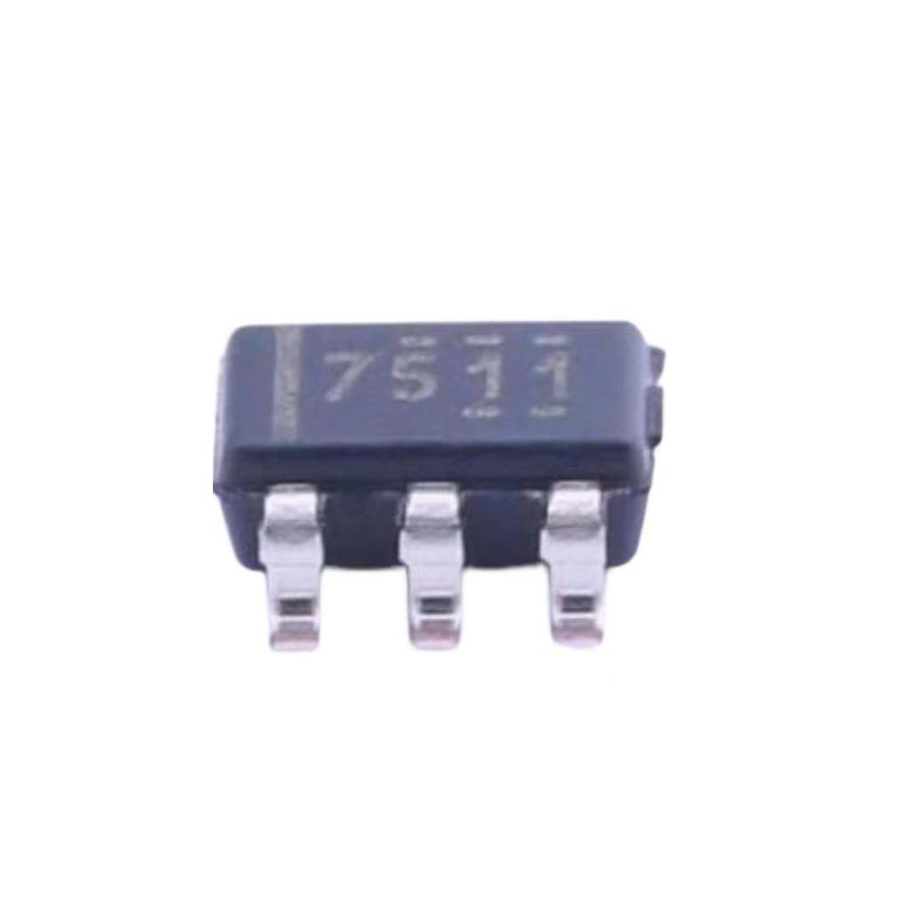

The UCC27511DBVR operates as a high-speed buffer amplifier between a low-power PWM controller and a high-power switching transistor (MOSFET, IGBT, or GaN FET).

Input Stage: The UCC27511 features a dual-input architecture with IN+ (non-inverting) and IN- (inverting) pins. The output state is determined by the logic AND of the two inputs: the output is HIGH when IN+ is HIGH and IN- is LOW, and the output is LOW in all other input combinations. This truth table allows the device to function as either an inverting or non-inverting driver, depending on which input receives the PWM signal and how the other input is biased. Internal pull-up (IN-) and pull-down (IN+) resistors ensure the output is held LOW when inputs are floating, providing a safe default state.

Input Threshold Logic: The input threshold levels are based on TTL/CMOS-compatible low-voltage logic and are fixed at approximately 1.2 V (LOW) and 2.2 V (HIGH), regardless of the VDD supply voltage. This means the UCC27511 can be driven directly from 3.3 V or 5 V logic signals even when VDD is 12 V or 15 V. The approximately 1 V hysteresis between the high and low thresholds provides excellent noise immunity, preventing false switching due to ground bounce or EMI coupling.

Output Stage: The UCC27511 features a split output configuration with OUTH and OUTL pins. The OUTH pin sources current through a hybrid pull-up structure consisting of a P-channel MOSFET in parallel with an N-channel MOSFET. The N-channel MOSFET is briefly turned on during the output rising edge to provide a boost in peak source current (the Gate Voltage Boost feature), reducing the effective source resistance during the Miller plateau region. The OUTL pin sinks current through an N-channel MOSFET pull-down structure with very low on-resistance. This asymmetric design provides 4 A peak source and 8 A peak sink capability.

Split Output Operation: The OUTH pin connects to the power switch gate through a turn-on gate resistor (RGO), and the OUTL pin connects through a turn-off gate resistor (RGOFF). During turn-on, OUTH drives current through RGO to charge the gate capacitance. During turn-off, OUTL sinks current through RGOFF to discharge the gate. By choosing RGO smaller than RGOFF, the turn-on can be fast (low switching loss) while the turn-off is slower (reducing voltage overshoot). Alternatively, choosing RGOFF smaller than RGO provides fast turn-off with slower turn-on.

UVLO Protection: The undervoltage lockout circuit monitors the VDD supply voltage. When VDD is below the UVLO threshold (approximately 4.5 V), the output is held LOW regardless of the input signals. This ensures that the power switch is not driven with insufficient gate voltage, which could cause it to operate in the linear region and overheat. The UVLO has approximately 350 mV of hysteresis to prevent chattering near the threshold.

Propagation Delay: The internal signal path from input to output is optimized for minimum propagation delay. The typical delay is 13 ns at VDD = 12 V, with very little variation across the VDD and temperature range (less than 20 ns under all conditions). This fast and consistent propagation delay minimizes pulse width distortion and dead-time requirements in bridge converter applications.

Shoot-Through Prevention: The output stage design inherently minimizes shoot-through current (simultaneous conduction of the pull-up and pull-down structures). The anti-shoot-through circuitry ensures a minimum dead time between the OUTH turning off and OUTL turning on (and vice versa), preventing excessive supply current spikes during output transitions.

Driving GaN FETs: The UCC27511 is particularly well-suited for driving enhancement-mode GaN FETs, which require low gate drive voltages (5-6 V), very fast switching speeds, and minimal parasitic inductance in the gate loop. The SOT-23-6 package has very low parasitic inductance, and the split output allows a 0 Ohm turn-on resistor (OUTH directly to gate) with a slightly larger turn-off resistor (OUTL through 1-2 Ohm) for optimal GaN switching performance.

Pin Name Type Description
1 OUTH Output Source output (pull-up); drives current into the power switch gate during turn-on; connect to gate through turn-on resistor (RGO); the output swings to VDD when active; 4 A peak source current; hybrid N-ch + P-ch MOSFET structure provides low effective source resistance; can be shorted to OUTL pin if separate turn-on/turn-off resistors are not needed
2 GND Ground Ground reference for the device; connect to PCB ground plane with low-inductance path; all output sink current returns through this pin; the ground connection must be as close to the power switch source terminal as possible to minimize gate loop inductance; bypass VDD to GND with 1 uF ceramic capacitor placed close to the pins
3 IN+ Input Non-inverting input; TTL/CMOS compatible threshold (LOW: below 1.2 V, HIGH: above 2.2 V); internal pull-down resistor (approximately 200 kOhm) holds the pin LOW when floating; the output follows IN+ when IN- is LOW; if IN+ is not used, connect to GND or leave floating (output will be LOW by default); input voltage range extends beyond VDD (not restricted by supply voltage)
4 IN- Input Inverting input; TTL/CMOS compatible threshold (same as IN+); internal pull-up resistor (approximately 200 kOhm) holds the pin HIGH when floating; the output is forced LOW when IN- is HIGH regardless of IN+; if IN- is not used, connect to GND to enable non-inverting operation; can be used as an active-low enable pin; input voltage range extends beyond VDD
5 VDD Power Supply voltage; 4.5 V to 18 V; determines the gate drive voltage amplitude (output swings from GND to VDD); bypass with a low-ESR 1 uF ceramic capacitor to GND placed within 5 mm of the pin; supply current is primarily the gate charge current (Qg x fsw) plus a small quiescent current (typically 150 uA); UVLO holds output LOW when VDD is below 4.5 V
6 OUTL Output Sink output (pull-down); sinks current from the power switch gate during turn-off; connect to gate through turn-off resistor (RGOFF); the output pulls to GND when active; 8 A peak sink current; low on-resistance N-channel MOSFET provides fast gate discharge; the strong sink capability prevents Miller turn-on in bridge configurations; can be shorted to OUTH pin for single-resistor gate drive
Application Description
Switch-Mode Power Supply (SMPS) Drive low-side MOSFET in buck, boost, or flyback converters; 4 A source quickly charges gate through Miller plateau; 8 A sink rapidly discharges gate preventing Miller turn-on; split output allows independent turn-on/turn-off speed optimization; 13 ns propagation delay supports high-frequency switching (100 kHz to 1 MHz); SOT-23-6 package fits easily near the MOSFET
Motor Drive Inverter Drive IGBT or MOSFET in three-phase motor drive bridge; 8 A sink current provides robust immunity against Miller turn-on during dead-time transitions; split output allows slower turn-off to reduce voltage overshoot on motor windings; dual-input supports inverting or non-inverting PWM signal from controller; -40 to 140 C operation handles motor drive thermal environment
GaN FET Driver Drive enhancement-mode GaN transistors in high-frequency (MHz) power converters; 5 V VDD provides correct gate drive voltage for GaN; 13 ns delay and 9 ns rise time match GaN switching speed; low-inductance SOT-23-6 package minimizes gate loop parasitics; split output with 0 Ohm RGO and 1-2 Ohm RGOFF provides optimal GaN turn-on/turn-off performance
DC-DC Converter Synchronous Buck Drive the low-side synchronous MOSFET in a synchronous buck converter; 8 A sink current ensures fast turn-off to prevent shoot-through during the high-side switch turn-on; split output allows different gate resistors for optimal switching loss vs. EMI tradeoff; low propagation delay minimizes dead-time requirement and reduces body diode conduction loss
Solar Inverter Drive MOSFETs or IGBTs in solar micro-inverter or string inverter; wide temperature range (-40 to 140 C) suits outdoor installations; split output allows adaptive gate drive with slower turn-off for reduced EMI; dual-input supports inverting configuration for active-low PWM controllers; UVLO ensures gate is not driven with insufficient voltage
Model Manufacturer Compatibility Key Difference
UCC27512DBVR TI Same Family, Single Output Single output version (OUT pin only, not split); 4 A source / 4 A sink symmetric drive; same dual-input, same package, same supply range; use when independent turn-on/turn-off control is not needed and 4 A sink is sufficient; lower cost alternative
UCC27531DBVR TI Similar, Single Input Single-channel gate driver with single input (non-inverting only); 4 A source / 8 A sink asymmetric drive; split output (OUTH/OUTL); same package and supply range; use when inverting input is not needed; slightly simpler design
NCP81074B ON Semi Functional Equivalent 4 A source / 8 A sink gate driver in SOT-23-6; similar split output; similar propagation delay; different pinout (not pin-compatible); use as alternative source; verify pin assignments before PCB layout
TC4420EOA Microchip Higher Current, Single Output 6 A single-output gate driver in SOIC-8; higher drive current; non-inverting only; larger package; no split output; use when 6 A drive is needed and split output is not required; not pin-compatible
IR4427S Infineon Dual Channel Alternative Dual low-side gate driver in SOIC-8; two independent channels; 1.5 A per channel; lower drive current; larger package; use when two gate drive channels are needed and 1.5 A per channel is sufficient
Recommend Parts
PMIC for AM335x, 3 bucks, 2 LDOs, battery charger, WLED, I2C, VQFN-48

Brand:

Package:

VQFN-48 (6×6 mm, 0.4 mm pitch)
In stock:
8909pcs

Cargo cycle: 3~7 Days
The minimum order is 1

Go to Inquiry
Octal D-type flip-flop, edge-triggered, async clear, 28MHz, SOP-20

Brand:

Package:

SOP-20 (NS) (12.6×7.8 mm)
In stock:
8359pcs

Cargo cycle: 3~7 Days
The minimum order is 1

Go to Inquiry
3-to-8 decoder/demux, active-low outputs, 3 enable inputs, 15ns, PDIP-16

Brand:

Package:

PDIP-16 (24.33×9.4 mm, Through-Hole)
In stock:
11952pcs

Cargo cycle: 3~7 Days
The minimum order is 1

Go to Inquiry
2W mono Class-AB audio amp, BTL speaker + SE headphone, 2.5-5.5V, HVSSOP-8

Brand:

Package:

HVSSOP-8 (DGN) (3.0×4.9 mm, PowerPAD)
In stock:
3337pcs

Cargo cycle: 3~7 Days
The minimum order is 1

Go to Inquiry
10/100 Ethernet PHY, MII/RMII/SNI, Auto-MDIX, 270mW, LQFP-48, commercial

Brand:

Package:

LQFP-48 (7×7 mm)
In stock:
14754pcs

Cargo cycle: 3~7 Days
The minimum order is 1

Go to Inquiry
Octal bus transceiver, 3-state outputs, 2-6V, 12ns tpd, TSSOP-20

Brand:

Package:

TSSOP-20 (6.5×6.4 mm)
In stock:
2638pcs

Cargo cycle: 3~7 Days
The minimum order is 1

Go to Inquiry
Quality Assurance

All electronic components we source from our partnered supply chains go through strict incoming inspections.Through careful testing, we ensure everything delivered to customers is genuine original parts and meets quality requirements.In addition, we keep complete inspection records to make the entire supply chain process clear and traceable.

Certification
We have obtained a number of professional certifications and built our own professional testing laboratory.This ensures that every product we deliver to our customers meets the highest quality requirements.We conduct tests in strict accordance with procedures to ensure stable product quality and accurate parameters.To guarantee genuine original parts, we also cooperate with reliable third-party testing institutions for strict quality inspection.We always attach great importance to quality and fully comply with industry standards, relevant regulations, and ISO 9001:2015 requirements.

Shipping & Payment

All electronic components we source from our partnered supply chains go through strict incoming inspections.Through careful testing, we ensure everything delivered to customers is genuine original parts and meets quality requirements.In addition, we keep complete inspection records to make the entire supply chain process clear and traceable.

Certification
We have obtained a number of professional certifications and built our own professional testing laboratory.This ensures that every product we deliver to our customers meets the highest quality requirements.We conduct tests in strict accordance with procedures to ensure stable product quality and accurate parameters.To guarantee genuine original parts, we also cooperate with reliable third-party testing institutions for strict quality inspection.We always attach great importance to quality and fully comply with industry standards, relevant regulations, and ISO 9001:2015 requirements.

Service & Packaging

All electronic components we source from our partnered supply chains go through strict incoming inspections.Through careful testing, we ensure everything delivered to customers is genuine original parts and meets quality requirements.In addition, we keep complete inspection records to make the entire supply chain process clear and traceable.

Certification
We have obtained a number of professional certifications and built our own professional testing laboratory.This ensures that every product we deliver to our customers meets the highest quality requirements.We conduct tests in strict accordance with procedures to ensure stable product quality and accurate parameters.To guarantee genuine original parts, we also cooperate with reliable third-party testing institutions for strict quality inspection.We always attach great importance to quality and fully comply with industry standards, relevant regulations, and ISO 9001:2015 requirements.



