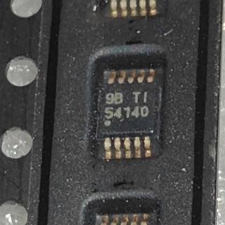
The TPS54140DGQR from Texas Instruments is a 42V, 1.5A step-down DC/DC converter with an integrated high-side N-channel MOSFET, designed for industrial, automotive aftermarket, and general-purpose power supply applications. The device uses current-mode control with a wide switching frequency range (100kHz to 2.5MHz), allowing designers to optimize the trade-off between efficiency and external component size.
The TPS54140A is an improved version of the original TPS54140, featuring a tighter enable threshold for more accurate undervoltage lockout (UVLO) programming. Both versions share the same pinout, package, and most electrical characteristics, and the TPS54140A is recommended for new designs. The DGQR suffix indicates the HVSSOP-EP (PowerPAD MSOP-10) package in tape-and-reel packaging.
Key features include a wide input voltage range (3.5V to 42V) that supports 12V and 24V industrial bus voltages with margin, a 200mohm integrated high-side MOSFET that delivers up to 1.5A continuous output current, and an adjustable output voltage from 0.8V to 39V using external resistors with a 0.8V internal reference. The wide output range allows the device to generate common logic voltages (1.8V, 2.5V, 3.3V, 5V) as well as intermediate voltages for specialized applications.
The Eco-mode pulse-skipping feature dramatically reduces quiescent current at light loads. When the output current drops below the Eco-mode threshold, the device enters a pulse-skipping mode where switching cycles are skipped to maintain regulation while minimizing switching losses. The no-load regulated supply current drops to 116uA, making the device suitable for always-on or standby power rails in battery-powered systems. When full PWM operation is needed for tight output voltage regulation or minimum output ripple, the Eco-mode can be defeated by keeping the load above the pulse-skipping threshold.
The adjustable switching frequency is set via an external resistor from the RT/CLK pin to GND. Lower frequencies (100-500kHz) improve efficiency by reducing switching losses but require larger inductors and capacitors. Higher frequencies (1-2.5MHz) allow smaller external components but increase switching losses. The RT/CLK pin also functions as a synchronization input, allowing the switching frequency to be synchronized to an external clock source. This is useful in systems with multiple converters where beat frequencies or electromagnetic interference (EMI) must be minimized.
The slow start (SS/TR) pin provides adjustable output voltage ramp-up time, preventing inrush current surges during startup. The pin can also be configured for power supply sequencing or tracking, where the output voltage follows a master rail with a defined ratio. This is critical in systems with FPGAs, processors, or other devices that require specific power-on sequencing.
The power-good (PWRGD) output is an open-drain transistor that pulls LOW when the output voltage falls outside the 94%-107% window of the nominal setpoint. This signal can be used to enable downstream loads, trigger fault handlers, or daisy-chain multiple converters for sequential power-up. The PWRGD pin has a built-in filter to prevent false triggering during transient events.
The EN (enable) pin serves a dual purpose: it enables/disables the converter, and it allows adjustable UVLO with hysteresis. The internal UVLO is set at 2.5V, but by connecting a resistor divider from VIN to EN, the UVLO threshold can be increased to any voltage up to 42V. The hysteresis is created by the difference between the EN rising threshold (1.25V) and falling threshold (1.11V), preventing chattering during slow input voltage ramps.





 English
  简体中文
简体中文  Español
  العربية