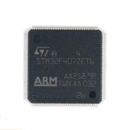
The STM32F207ZET operates as a 32-bit ARM Cortex-M3 microcontroller with a sophisticated multi-bus architecture optimized for high throughput and deterministic real-time performance.
ARM Cortex-M3 Core: The Cortex-M3 processor features a 3-stage pipeline, hardware division (2-12 cycles), single-cycle multiply, bit-band support for atomic bit manipulation, and a Nested Vectored Interrupt Controller (NVIC) with up to 81 interrupt channels and 16 priority levels. The built-in Memory Protection Unit (MPU) allows privileged software to define memory regions with access permissions, enabling operating system implementations like RTOS to isolate tasks. The core supports two operating modes (Thread and Handler) and two privilege levels, providing a foundation for secure embedded software.
ART Accelerator: The ART Accelerator is a critical performance enabler. Flash memory access at 120 MHz normally requires wait states (3-4 cycles for 90nm Flash at 120 MHz). The ART Accelerator uses a 64-line instruction cache, an 8-line literal cache, and a 64-line branch cache (with branch folding) to hide Flash wait states. When the access pattern hits in the accelerator cache, the CPU sees zero-wait-state performance. ST benchmarks demonstrate 150 DMIPS and 398 CoreMark, which is the theoretical maximum for Cortex-M3 at 120 MHz. Without ART, the same CPU would deliver approximately 115 DMIPS due to Flash wait states.
Multi-AHB Bus Matrix: The STM32F207 employs an 8-master, 7-slave multi-AHB bus matrix connecting the CPU D-bus, I-bus, and S-bus, DMA1, DMA2, Ethernet DMA, USB HS DMA, and the DMA of the camera interface to memories and peripherals. The bus matrix allows concurrent accesses from multiple masters to different slaves (e.g., CPU fetching code from Flash while DMA reads SRAM), significantly increasing sustained throughput. The matrix runs at the full AHB frequency (120 MHz), providing 480 MB/s bandwidth per master port.
Memory Subsystem: The 512 KB Flash is organized as 2 KB sectors (4 KB for the first 4 sectors) supporting erase/program operations. The 128 KB SRAM is split into 112 KB main SRAM (0x20000000) accessible by all bus masters, and 16 KB Core-Coupled Memory (CCM, 0x10000000) accessible only by the CPU D-bus at full speed with zero-wait-state access. The CCM is ideal for time-critical data, stack, or ISR code. The 4 KB backup SRAM in the VBAT domain retains data even in Standby mode.
DMA Controller: The 16-stream DMA controller with dedicated FIFOs supports burst transfers (4/8/16 beats), circular mode, and double-buffer mode. Each stream can be configured with priority levels and supports memory-to-memory, memory-to-peripheral, and peripheral-to-memory transfers. The centralized FIFOs allow the DMA to absorb latency mismatches between source and destination, preventing data loss in high-speed peripherals like SPI at 30 Mbit/s.
Ethernet MAC: The 10/100 Ethernet MAC implements IEEE 802.3 with dedicated DMA and FIFO. The MII/RMII interface connects to an external PHY. IEEE 1588v2 hardware support provides sub-microsecond time stamping for precision time protocol (PTP) applications. The DMA descriptor ring architecture supports scatter-gather DMA, reducing CPU intervention in packet processing.
Power Management: The internal voltage regulator steps 1.8-3.6V VDD down to 1.2V for the core. Dynamic voltage scaling is not available on F2 (it is on F4), but the device supports Sleep (CPU halted, peripherals running), Stop (all clocks stopped, SRAM and register contents preserved), and Standby (only RTC and backup domain alive, SRAM lost) modes. VBAT supply (1.65-3.6V) maintains the RTC, 20 backup registers, and 4 KB backup SRAM when VDD is removed.





 English
  简体中文
简体中文  Español
  العربية