Home > Integrated Circuits ICs > STM32F030K6T6TR

STM32F030K6T6TR


ARM Cortex-M0 MCU, 48MHz, 32KB Flash, 4KB SRAM, 12-bit ADC, I2C/SPI/USART, LQFP-32, 2.4-3.6V, -40~85C

49737

Effective Inventory
Go to Inquiry

Image for reference only

Manufacturer Part:

STM32F030K6T6TR

Package:

LQFP-32 (7 x 7 x 1.4 mm, 0.8mm pitch)

Brand:
Product Categories:
Other recommendations you may be interested in.
Description

The STM32F030K6T6TR from STMicroelectronics is an entry-level ARM Cortex-M0 32-bit microcontroller in a 32-pin LQFP package (7 x 7 x 1.4 mm). Key specifications: ARM Cortex-M0 core at up to 48 MHz; 32 Kbytes Flash memory; 4 Kbytes SRAM with hardware parity; CRC calculation unit; 26 GPIO pins (most 5V tolerant); 12-bit ADC with 10 channels (1.0 us conversion time, 0-3.6V range); 5x 16-bit timers + 1x advanced-control PWM timer; 1x I2C (Standard/Fast/Fast Mode Plus up to 1Mbit/s, SMBus); 1x SPI (18 Mbit/s, 4-16 bit frame); 1x USART (with auto baud rate detection, master synchronous SPI mode); 1x DMA controller (5 channels); RTC with calendar and alarm; 2x watchdog timers (independent and window); SysTick timer; Serial Wire Debug (SWD) interface. Supply voltage: 2.4V to 3.6V. Power modes: Run, Sleep, Stop, Standby. Clock sources: 4-32 MHz HSE crystal, 32 kHz LSE crystal, 8 MHz HSI RC (with PLL up to 48 MHz), 40 kHz LSI RC. Operating temperature: -40C to +85C. The TR suffix indicates tape-and-reel packaging (vs tray for T6 suffix). Active product, ECOPACK2 (RoHS compliant), ECCN 3A991a.2.

The STM32F030K6T6TR from STMicroelectronics is an entry-level 32-bit microcontroller based on the ARM Cortex-M0 core, offering 32 Kbytes of Flash memory and 4 Kbytes of SRAM in a compact 32-pin LQFP package. It is the value-line product in the STM32F0 series, designed to provide the benefits of 32-bit ARM processing at price points competitive with 8-bit microcontrollers.

The STM32F030K6 targets applications that require more processing power and peripheral sophistication than 8-bit MCUs can provide, but at minimal cost. The ARM Cortex-M0 core delivers up to 48 MHz clock frequency with 0.95 DMIPS/MHz performance, providing roughly 10x the processing power of a typical 8-bit MCU running at the same clock frequency. This performance advantage enables more complex algorithms, faster response times, and more sophisticated control strategies.

The 32 Kbytes of Flash and 4 Kbytes of SRAM provide adequate memory for many embedded applications: sensor data acquisition and processing, motor control, user interface management, communication protocol handling, and general-purpose control. The hardware parity on SRAM enhances data integrity, which is important for safety-critical and industrial applications.

The peripheral set is remarkably complete for a value-line MCU. The 12-bit ADC with 1.0 us conversion time provides fast and accurate analog measurement. The I2C interface supports Fast Mode Plus (1 Mbit/s) with 20 mA output drive, enabling direct connection to I2C buses without external buffers. The SPI interface supports frame sizes from 4 to 16 bits, accommodating non-standard SPI peripherals. The USART interface includes auto baud rate detection, simplifying communication with devices at unknown baud rates.

The five 16-bit timers plus one advanced-control PWM timer provide extensive timing and PWM generation capabilities. The advanced-control timer (TIM1) supports six-channel PWM output with complementary outputs and dead-time insertion, making it suitable for motor drive and power conversion applications. The general-purpose timers support input capture, output compare, and PWM generation for a wide range of timing functions.

The LQFP-32 package provides 26 GPIO pins, which is sufficient for most applications that use the available peripherals. Most GPIO pins are 5V tolerant, meaning they can accept input voltages up to 5.5V even when VDD is 3.3V. This simplifies interfacing with 5V logic devices and protects against voltage spikes on input lines.

The clock system is flexible, with four clock sources: a 4-32 MHz high-speed external (HSE) crystal for precision timing, a 32 kHz low-speed external (LSE) crystal for RTC calibration, an 8 MHz high-speed internal (HSI) RC oscillator with PLL for cost-sensitive applications, and a 40 kHz low-speed internal (LSI) RC oscillator for independent watchdog and RTC backup. The PLL can multiply the HSE or HSI clock to achieve the maximum 48 MHz system clock.

The power management features include four operating modes: Run (full operation), Sleep (CPU stopped, peripherals running), Stop (all clocks stopped, SRAM and register content retained), and Standby (minimum power, only RTC and backup registers retained). These modes allow the designer to optimize power consumption for battery-powered applications.

The STM32F030K6 is part of the STM32 ecosystem, which provides extensive development tools, middleware libraries, and application examples. The STM32CubeMX configuration tool generates initialization code, and the STM32CubeF0 HAL/LL libraries provide a comprehensive software framework. The Serial Wire Debug (SWD) interface supports real-time debugging and flash programming through low-cost debug probes such as ST-Link.

The TR suffix indicates tape-and-reel packaging, suitable for automated SMT assembly. The T6 suffix (without R) indicates tray packaging. Both have identical electrical specifications and are available in the industrial temperature grade (-40C to +85C).
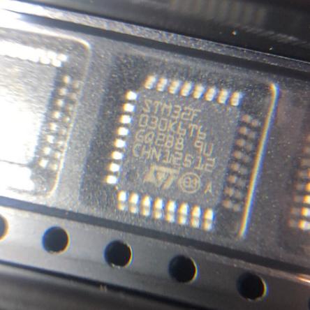

The STM32F030K6T6TR operates as a 32-bit ARM Cortex-M0 microcontroller with on-chip Flash, SRAM, and peripherals.

ARM Cortex-M0 Core: The Cortex-M0 is a 32-bit RISC processor core that implements the ARMv6-M architecture. It provides a subset of the Thumb-2 instruction set, supporting 16-bit and 32-bit instructions for optimal code density. The core includes 13 general-purpose 32-bit registers, a program counter, a link register, a program status register, and a stack pointer. The processor has a 3-stage pipeline (Fetch, Decode, Execute) and can execute most single-cycle instructions. The Nested Vectored Interrupt Controller (NVIC) supports up to 32 interrupt channels with 4 programmable priority levels, providing fast and deterministic interrupt handling.

Memory Architecture: The 32 Kbytes of Flash memory stores the program code and constant data. Flash is organized as 1 Kbyte pages and supports in-circuit programming (ICP) via SWD and in-application programming (IAP) via software. The 4 Kbytes of SRAM with hardware parity detection stores variables, stack, and dynamic data. The parity checking generates a non-maskable interrupt (NMI) when a parity error is detected, enhancing data integrity in safety-critical applications.

Bus Matrix: The AHB (Advanced High-performance Bus) bus matrix connects the Cortex-M0 core, DMA controller, and SRAM to the Flash memory and peripheral bridges. The APB (Advanced Peripheral Bus) bridges connect the AHB bus to the peripheral registers. The DMA controller (5 channels) can transfer data between peripherals and SRAM without CPU intervention, freeing the CPU for computation tasks.

Clock System: The clock control unit (RCC) manages all clock sources and distribution. The system clock (SYSCLK) can be sourced from HSI (8 MHz RC), HSE (4-32 MHz crystal), or PLL output. The PLL can multiply HSI/8 or HSE by a factor of 2-16, achieving up to 48 MHz. The AHB prescaler divides SYSCLK for the CPU, DMA, and memory bus. The APB prescalers further divide the AHB clock for the peripherals. The clock security system (CSS) can detect HSE failure and automatically switch to HSI, preventing system lockup.

Power Management: The power controller manages the four operating modes. In Run mode, all clocks and peripherals are active. In Sleep mode (entered by WFI/WFE instruction), the CPU clock stops but peripheral clocks continue. In Stop mode (entered by WFI with PDDS=0 and LPDS=1), all oscillators stop but SRAM content is preserved; wake-up is triggered by any external interrupt. In Standby mode (entered by WFI with PDDS=1), only the RTC, IWDG, and backup registers remain powered; wake-up is triggered by NRST, IWDG reset, or RTC alarm. The power-on reset (POR) and power-down reset (PDR) circuits ensure clean startup when VDD ramps up or down.

ADC Operation: The 12-bit successive approximation ADC converts analog input voltages (0 to 3.6V) to digital values in 1.0 us. The ADC supports single, continuous, scan, and discontinuous conversion modes. DMA transfers can automate the conversion sequence, storing results directly to SRAM without CPU intervention. The analog watchdog can generate an interrupt when the conversion result falls outside a programmed window.

Debug Interface: The Serial Wire Debug (SWD) interface uses two pins (SWDIO and SWCLK) to provide real-time debugging capabilities including breakpoints, watchpoints, and register/memory access. The SWD interface also supports flash programming, allowing firmware updates without removing the device from the circuit. The debug interface is compatible with ST-Link and other ARM SWD debug probes.

Pin Name Type Description
1 VDD Power Digital power supply; 2.4V to 3.6V; connect to 3.3V rail with 100nF decoupling capacitor to VSS; all VDD pins must be connected together externally
2 PF0-OSC_IN I/O (FT) General-purpose I/O or HSE oscillator input; after reset = PF0; alternate function: I2C1_SDA, OSC_IN; 5V tolerant
3 PF1-OSC_OUT I/O (FT) General-purpose I/O or HSE oscillator output; after reset = PF1; alternate function: I2C1_SCL, OSC_OUT; 5V tolerant
4 NRST I/O (RST) Reset pin; active-low bidirectional reset with internal pull-up; input: external reset assertion; output: internal reset pulse (e.g., watchdog, power-on); connect 100nF capacitor to GND for noise filtering; do not add external pull-up (internal already present)
5 VDDA Power Analog power supply for ADC, reset, and clock; must be between VDD and 3.6V; connect to VDD with 100nF and 1uF decoupling capacitors; separate from digital VDD for best ADC performance; can be connected to VDD if ADC performance is not critical
6 PA0 I/O (TTa) General-purpose I/O; 3.3V tolerant, directly connected to ADC channel 0; alternate functions: USART4_TX, TIM1_BKIN; ADC input (0-3.6V)
7 PA1 I/O (TTa) General-purpose I/O; ADC channel 1; alternate functions: USART4_RX, TIM1_CH1, EVENTOUT
8 PA2 I/O (TTa) General-purpose I/O; ADC channel 2; alternate functions: USART1_TX, TIM1_CH2, TIM15_CH1, EVENTOUT
9 PA3 I/O (TTa) General-purpose I/O; ADC channel 3; alternate functions: USART1_RX, TIM1_CH3, TIM15_CH2, EVENTOUT
10 PA4 I/O (TTa) General-purpose I/O; ADC channel 4; alternate functions: SPI1_NSS, USART2_CK, TIM14_CH1, EVENTOUT
11 PA5 I/O (TTa) General-purpose I/O; ADC channel 5; alternate functions: SPI1_SCK, TIM2_CH1, TIM14_CH1, EVENTOUT
12 PA6 I/O (TTa) General-purpose I/O; ADC channel 6; alternate functions: SPI1_MISO, TIM1_BKIN, TIM3_CH1, TIM16_CH1, EVENTOUT
13 PA7 I/O (TTa) General-purpose I/O; ADC channel 7; alternate functions: SPI1_MOSI, TIM1_CH1N, TIM3_CH2, TIM14_CH1, TIM17_CH1, EVENTOUT
14 PB0 I/O (TTa) General-purpose I/O; ADC channel 8; alternate functions: TIM1_CH2N, TIM3_CH3, EVENTOUT
15 PB1 I/O (TTa) General-purpose I/O; ADC channel 9; alternate functions: TIM1_CH3N, TIM3_CH4, TIM14_CH1, EVENTOUT
16 VSS Ground Digital ground; connect to PCB ground plane; all VSS pins must be connected together externally
17 VDD Power Digital power supply (second pin); must be connected to same supply as Pin 1
18 PB8 I/O (FT) General-purpose I/O; 5V tolerant; alternate functions: I2C1_SCL, TIM16_CH1, EVENTOUT; also serves as BOOT0 function when configured
19 PB9 I/O (FT) General-purpose I/O; 5V tolerant; alternate functions: I2C1_SDA, TIM17_CH1, EVENTOUT
20 BOOT0 Input (B) Boot configuration pin; determines boot source after reset; LOW (0) = boot from Main Flash (normal operation); HIGH (1) = boot from System Memory (bootloader for UART/SWD programming); connect with 10k pull-down to GND for normal operation; add jumper or switch to VDD for programming mode; do not leave floating
21 PB7 I/O (FT) General-purpose I/O; 5V tolerant; alternate functions: I2C1_SDA, TIM17_CH1N, TIM4_CH2, EVENTOUT
22 PB6 I/O (FT) General-purpose I/O; 5V tolerant; alternate functions: I2C1_SCL, TIM16_CH1N, TIM4_CH1, EVENTOUT
23 VSS Ground Digital ground (second pin)
24 VDD Power Digital power supply (third pin)
25 PB5 I/O (FT) General-purpose I/O; 5V tolerant; alternate functions: SPI1_MOSI, I2C1_SMBA, TIM3_CH2, TIM16_BKIN, EVENTOUT
26 PB4 I/O (FT) General-purpose I/O; 5V tolerant; alternate functions: SPI1_MISO, TIM3_CH1, TIM17_BKIN, EVENTOUT
27 PB3 I/O (FT) General-purpose I/O; 5V tolerant; alternate functions: SPI1_SCK, EVENTOUT
28 PD2 I/O (FT) General-purpose I/O; 5V tolerant; alternate functions: TIM3_ETR, EVENTOUT
29 PA12 I/O (FT) General-purpose I/O; 5V tolerant; alternate functions: USART1_RTS, TIM1_ETR, EVENTOUT
30 PA11 I/O (FT) General-purpose I/O; 5V tolerant; alternate functions: USART1_CTS, TIM1_CH4, EVENTOUT
31 PA10 I/O (FT) General-purpose I/O; 5V tolerant; alternate functions: USART1_RX, TIM1_CH3, TIM17_BKIN, EVENTOUT
32 PA9 I/O (FT) General-purpose I/O; 5V tolerant; alternate functions: USART1_TX, TIM1_CH2, TIM15_BKIN, EVENTOUT
Application Description
Low-Cost Sensor Node Acquire sensor data via 12-bit ADC (10 channels, 1us conversion), process with Cortex-M0 at 48MHz, and transmit via USART or SPI; 32KB Flash sufficient for sensor drivers and communication stacks; 4KB SRAM for data buffering; low cost competitive with 8-bit MCUs; STM32CubeMX simplifies peripheral configuration
Simple Motor Control Drive BLDC or stepper motors using TIM1 advanced-control timer with 6-channel PWM and dead-time insertion; 12-bit ADC reads motor current and position sensors; I2C interface for motor driver IC communication; 32KB Flash stores motor control algorithms; cost-effective alternative to dedicated motor control MCUs
Home Automation Controller Control home automation devices via I2C (sensors), SPI (displays), and USART (wireless modules); RTC provides time-stamping for events; low-power Stop mode between events preserves battery; 26 GPIO pins control relays, LEDs, and switches; SWD interface enables field firmware updates
Industrial Sensor Interface Interface with 4-20mA or 0-10V industrial sensors via 12-bit ADC; process data and transmit via USART (RS-485) or I2C (SMBus); watchdog timers ensure system reliability; -40C to +85C industrial temperature range; hardware CRC for data integrity in communication
8-bit MCU Replacement Replace 8-bit MCUs (PIC, AVR, 8051) with 32-bit performance at similar cost; Cortex-M0 at 48MHz delivers 10x processing power over 8-bit at same clock; Thumb instruction set provides excellent code density; STM32 ecosystem provides free tools and libraries; easy migration path to higher-end STM32 devices
Model Manufacturer Compatibility Key Difference
STM32F030K6T6 ST Same, Tray Package Identical electrical specifications; T6 suffix = tray packaging (1500 units/tray) for manual or automated placement; TR suffix = tape and reel for automated SMT assembly; same LQFP-32 package; use TR for production, T6 for prototyping
STM32F030C6T6 ST More Pins Same Cortex-M0, 32KB Flash, 4KB SRAM but in LQFP-48 package; 38 GPIO pins (vs 26); additional peripherals: 2x I2C, 2x SPI, 2x USART; more ADC channels; same core and memory; use when more I/O or communication interfaces are needed
STM32F030F4P6 ST Smaller, Less Memory Same Cortex-M0 core but 16KB Flash, 4KB SRAM in TSSOP-20 (4.4×6.5mm); 15 GPIO pins; 1x I2C, 1x USART, 1x SPI; fewer timers; lower cost; use for cost-sensitive applications with minimal peripheral requirements
STM32G030K6T6 ST Newer Generation Cortex-M0+ at 64MHz; 32KB Flash, 8KB SRAM in LQFP-32; 12-bit ADC at 2.5Msps; USART with FIFO; same pinout family; more performance and features; use for new designs requiring more capability in same footprint
LPC824M201JHI33 NXP Competitive Alternative Cortex-M0+ at 30MHz; 32KB Flash, 8KB SRAM in HVQFN-33; 4x USART, 2x SPI, 1x I2C; switch matrix for flexible pin routing; different package and pinout; use as alternative ARM Cortex-M0 MCU
Recommend Parts
Cortex-M0+ ultra-low-power MCU, 32MHz, 128KB Flash, crystal-less USB, LQFP-64

Brand:

Package:

LQFP-64 (10×10 mm)
In stock:
14446pcs

Cargo cycle: 3~7 Days
The minimum order is 1

Go to Inquiry
Cortex-M4F MCU, 168MHz, 512KB Flash, 192KB SRAM, Ethernet, USB OTG, LQFP-100

Brand:

Package:

LQFP-100 (14×14×1.4 mm)
In stock:
2870pcs

Cargo cycle: 3~7 Days
The minimum order is 1

Go to Inquiry
ARM Cortex-M4F MCU, 72MHz, 384KB Flash, 64KB SRAM, dual ADC, 4 comparators, 2 op amps, LQFP-100

Brand:

Package:

LQFP-100 (14 x 14 x 1.4 mm)
In stock:
12274pcs

Cargo cycle: 3~7 Days
The minimum order is 1

Go to Inquiry
ARM Cortex-M4F MCU, 168MHz, 1MB Flash, 192KB SRAM, Ethernet, USB OTG HS, UFBGA-176

Brand:

Package:

UFBGA-176 (10 x 10 mm, 0.65mm pitch)
In stock:
9303pcs

Cargo cycle: 3~7 Days
The minimum order is 1

Go to Inquiry
Quad JFET-input op amp, 4MHz GBP, 16V/µs slew rate, 200pA bias current, SOIC-14

Brand:

Package:

SOIC-14 (8.75 x 4 x 1.65 mm)
In stock:
9834pcs

Cargo cycle: 3~7 Days
The minimum order is 1

Go to Inquiry
Ultra-low-power Cortex-M3 MCU, 32MHz, 256KB Flash, 32KB SRAM, LCD controller, LQFP-64

Brand:

Package:

LQFP-64 (10x10mm)
In stock:
5417pcs

Cargo cycle: 3~7 Days
The minimum order is 1

Go to Inquiry
Quality Assurance

All electronic components we source from our partnered supply chains go through strict incoming inspections.Through careful testing, we ensure everything delivered to customers is genuine original parts and meets quality requirements.In addition, we keep complete inspection records to make the entire supply chain process clear and traceable.

Certification
We have obtained a number of professional certifications and built our own professional testing laboratory.This ensures that every product we deliver to our customers meets the highest quality requirements.We conduct tests in strict accordance with procedures to ensure stable product quality and accurate parameters.To guarantee genuine original parts, we also cooperate with reliable third-party testing institutions for strict quality inspection.We always attach great importance to quality and fully comply with industry standards, relevant regulations, and ISO 9001:2015 requirements.

Shipping & Payment

All electronic components we source from our partnered supply chains go through strict incoming inspections.Through careful testing, we ensure everything delivered to customers is genuine original parts and meets quality requirements.In addition, we keep complete inspection records to make the entire supply chain process clear and traceable.

Certification
We have obtained a number of professional certifications and built our own professional testing laboratory.This ensures that every product we deliver to our customers meets the highest quality requirements.We conduct tests in strict accordance with procedures to ensure stable product quality and accurate parameters.To guarantee genuine original parts, we also cooperate with reliable third-party testing institutions for strict quality inspection.We always attach great importance to quality and fully comply with industry standards, relevant regulations, and ISO 9001:2015 requirements.

Service & Packaging

All electronic components we source from our partnered supply chains go through strict incoming inspections.Through careful testing, we ensure everything delivered to customers is genuine original parts and meets quality requirements.In addition, we keep complete inspection records to make the entire supply chain process clear and traceable.

Certification
We have obtained a number of professional certifications and built our own professional testing laboratory.This ensures that every product we deliver to our customers meets the highest quality requirements.We conduct tests in strict accordance with procedures to ensure stable product quality and accurate parameters.To guarantee genuine original parts, we also cooperate with reliable third-party testing institutions for strict quality inspection.We always attach great importance to quality and fully comply with industry standards, relevant regulations, and ISO 9001:2015 requirements.



