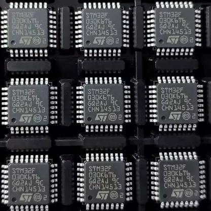
STM32F030K6T6


ARM Cortex-M0 MCU 48MHz, 32KB Flash, 4KB SRAM, 12-bit ADC, 1xI2C/SPI/USART, SWD, LQFP-32, -40~85C

30000

Effective Inventory
Go to Inquiry

Image for reference only

Manufacturer Part:

STM32F030K6T6

Package:

LQFP-32 (7 x 7 x 1.4 mm, 0.8mm pitch)

Brand:
Other recommendations you may be interested in.
Description

The STM32F030K6T6 from STMicroelectronics is a mainstream ARM Cortex-M0 32-bit RISC microcontroller operating at up to 48 MHz, featuring 32 KB Flash memory and 4 KB SRAM with hardware parity, in a 32-pin LQFP (7 x 7 x 1.4 mm) package. Key specifications: ARM Cortex-M0 core at 48 MHz; 32 KB Flash program memory; 4 KB SRAM; CRC calculation unit; supply voltage VDD 2.4 V to 3.6 V, VDDA VDD to 3.6 V; power-on and power-down reset (POR/PDR); low-power modes (Sleep, Stop, Standby); 4 to 32 MHz crystal oscillator; 32 kHz RTC oscillator with calibration; internal 8 MHz RC with x6 PLL option; internal 40 kHz RC oscillator; 26 fast I/O pins with 5 V tolerant capability on most pins; all I/O mappable to external interrupt vectors; 5-channel DMA controller; one 12-bit ADC with 1.0 us conversion time and up to 12 channels (conversion range 0 to 3.6 V); one 16-bit advanced-control timer (TIM1) with six-channel PWM output; multiple 16-bit general-purpose timers (TIM3, TIM14, TIM16, TIM17); independent watchdog (IWDG) and window watchdog (WWDG); SysTick timer; one I2C interface (Fast Mode Plus 1 Mbit/s capable, SMBus/PMBus support); one SPI interface (18 Mbit/s, 4 to 16 programmable bit frames); one USART supporting master synchronous SPI and modem control with auto baud rate detection; calendar RTC with alarm and periodic wakeup from Stop/Standby; serial wire debug (SWD); operating temperature -40 to +85 degrees C. ECOPACK2 compliant (RoHS). Active product status.

The STM32F030K6T6 is a member of the STM32F030x4/x6/x8/xC family of value-line ARM Cortex-M0 microcontrollers from STMicroelectronics. It represents the mid-density member (x6 = 32 KB Flash) in the smallest LQFP package option (32 pins), offering an optimal balance of cost, performance, and pin count for cost-sensitive embedded applications.

The STM32F030 series is ST’s entry-level ARM Cortex-M0 product line, designed to provide 32-bit performance at 8-bit microcontroller price points. The Cortex-M0 core delivers 0.84 DMIPS/MHz, providing approximately 40 DMIPS at the maximum 48 MHz clock frequency. This is significantly more processing power than 8-bit alternatives (e.g., ATmega328P at 20 MHz delivers approximately 20 MIPS), enabling more complex control algorithms and faster response times.

The 32 KB Flash and 4 KB SRAM provide adequate memory for typical embedded control applications: sensor interfacing, motor control, communication protocol handling, and user interface management. The hardware parity on SRAM enhances data integrity for safety-critical applications. The CRC calculation unit offloads firmware integrity checks from the CPU, useful for communication protocol verification and flash memory validation.

The 12-bit ADC with 1.0 us conversion time (1 Msps) and up to 12 channels covers most analog sensing requirements. The 1 Msps sampling rate is fast enough for single-phase current sensing in motor control applications, while the 12-bit resolution provides adequate precision for temperature, voltage, and current measurements. The ADC supports DMA transfers, allowing continuous conversion without CPU intervention.

The peripheral set (1x I2C, 1x SPI, 1x USART) is sufficient for most simple embedded systems. The I2C supports Fast Mode Plus (1 Mbit/s) for high-speed sensor communication. The SPI supports 18 Mbit/s for fast display or flash memory interfacing. The USART supports auto baud rate detection, simplifying communication with devices that use different baud rates.

The advanced-control timer (TIM1) with six-channel PWM output is a key differentiator for motor control and power conversion applications. It supports complementary PWM outputs with dead-time insertion, break input for fault protection, and center-aligned PWM mode for lower harmonic content in motor drive waveforms.

The LQFP-32 package with 26 usable I/O pins (6 pins are dedicated to power, ground, NRST, and BOOT0) provides enough connectivity for typical applications while maintaining a small 7 x 7 mm footprint. Most I/O pins are 5 V tolerant, allowing direct connection to 5 V logic devices without level shifting.

The comprehensive power management (Sleep, Stop, Standby modes) enables battery-powered applications. In Stop mode with RTC running, the current consumption drops to approximately 5.5 uA, making it suitable for periodic wakeup applications such as sensor nodes and data loggers.

At $0.87 per unit in volume (1000+), the STM32F030K6T6 is one of the most cost-effective 32-bit ARM microcontrollers on the market. Combined with the free STM32Cube development ecosystem (HAL drivers, CMSIS support, STM32CubeMX configuration tool) and the widespread availability of ARM development tools (Keil, IAR, GCC), it provides the lowest total cost of ownership for 32-bit embedded designs.

The STM32F030K6T6 operates as a complete 32-bit embedded microcontroller system on a single chip, integrating the ARM Cortex-M0 processor core with Flash memory, SRAM, and a comprehensive set of peripherals.

ARM Cortex-M0 Core: The Cortex-M0 is a 32-bit RISC processor core implementing the ARMv6-M architecture. It executes a subset of the Thumb instruction set (56 instructions), providing a good balance of code density and performance. The core features a 3-stage pipeline (Fetch, Decode, Execute) and can execute most instructions in a single clock cycle at 48 MHz. The Cortex-M0 includes a nested vectored interrupt controller (NVIC) that supports up to 32 external interrupt sources with configurable priority levels (4 priority levels for the STM32F030). The NVIC provides automatic context saving and restoring on interrupt entry and exit, reducing interrupt latency to a deterministic 16 clock cycles.

Memory Architecture: The 32 KB Flash memory stores the program code and constant data. It is organized as 1 KB pages and supports in-circuit programming (ICP) via SWD and in-application programming (IAP) for firmware updates. The Flash has an access time of 1 wait state at 48 MHz. The 4 KB SRAM stores variables, stack, and heap data. The SRAM has hardware parity checking that generates a parity fault exception on detection of a single-bit error, enhancing data integrity. The CRC calculation unit computes a 32-bit CRC on any memory region, useful for verifying Flash contents and communication data integrity.

Clock System: The STM32F030K6T6 has a flexible clock system with multiple clock sources. The internal 8 MHz RC oscillator provides a default clock at startup without any external components. The internal PLL can multiply the 8 MHz RC (or external crystal) by 6 to achieve 48 MHz. The external crystal oscillator supports 4 to 32 MHz crystals for applications requiring precise timing. The internal 40 kHz RC oscillator drives the independent watchdog. A 32.768 kHz crystal can be connected for the RTC, which provides calendar functions with alarm and periodic wakeup capability.

Power Management: The microcontroller supports three low-power modes. Sleep mode stops the CPU but keeps peripherals running; any interrupt wakes the CPU. Stop mode stops the CPU, all clocks, and most peripherals; only the RTC, IWDG, and external interrupts can cause wakeup; current consumption is approximately 5.5 uA. Standby mode is the lowest power mode, keeping only the RTC, IWDG, and backup registers alive; wakeup requires an external reset or RTC alarm; current consumption is approximately 2.8 uA.

Reset and Boot: The power-on reset (POR) and power-down reset (PDR) circuits ensure the MCU starts reliably when VDD rises above the threshold and holds the MCU in reset when VDD falls below the threshold. The BOOT0 pin selects the boot source at reset: when LOW (default), the MCU boots from Flash memory; when HIGH, the MCU boots from system memory (built-in bootloader supporting UART programming). The NRST pin is an active-low reset input with a built-in pull-up resistor.

Interrupt System: The NVIC supports up to 32 maskable interrupt channels with 4 programmable priority levels. All 26 I/O pins can be mapped to external interrupts (EXTI), supporting rising edge, falling edge, or both edge triggering. The EXTI also supports an interrupt from the RTC alarm and the internal voltage reference.

DMA Controller: The 5-channel DMA controller can transfer data between peripherals and memory (or memory to memory) without CPU intervention. Each channel can be configured for source/destination addresses, transfer width, and transfer count. The DMA supports circular mode for continuous ADC sampling and SPI communication.

Debug Interface: The serial wire debug (SWD) interface provides a 2-pin (SWDIO, SWCLK) connection for in-circuit debugging and Flash programming. SWD is compatible with ST-Link, J-Link, and other ARM debug probes. The debug interface supports breakpoints, watchpoints, single-step execution, and real-time variable monitoring.

Pin Name Type Description
1 VDD Power Digital power supply; 2.4 V to 3.6 V; must be decoupled with 100 nF ceramic capacitor plus 4.7 uF bulk capacitor; connect to 3.3 V supply; all VDD pins must be connected together externally
2 PF0 / OSC_IN I/O GPIO Port F pin 0; alternate function: external 4-32 MHz crystal oscillator input; 5 V tolerant; can be used as general-purpose I/O when crystal oscillator is not used; connect crystal between OSC_IN and OSC_OUT with load capacitors to GND
3 PF1 / OSC_OUT I/O GPIO Port F pin 1; alternate function: external crystal oscillator output; 5 V tolerant; can be used as general-purpose I/O when crystal oscillator is not used
4 NRST Input Active-low reset input with internal pull-up; asserting LOW for at least 20 ns generates a system reset; open-drain output during reset (can be driven by external reset source); connect 100 nF capacitor to GND for noise filtering; do not add external pull-up (internal pull-up is sufficient)
5 VDDA Power Analog power supply for ADC and reset blocks; 2.4 V to 3.6 V; must be connected to VDD or a filtered version of VDD; decouple with 100 nF ceramic capacitor plus 1 uF bulk capacitor; connect to VDD through a ferrite bead for improved ADC noise performance
6-7 PA0-PA1 I/O GPIO Port A pins 0-1; 5 V tolerant; alternate functions include ADC inputs (ADC_IN0-1), TIM2 CH1-2, TIM16 CH1, USART2, EXTI lines; PA0 also serves as WKUP pin for wakeup from Standby mode
8 PA2 / USART1_TX I/O GPIO Port A pin 2; 5 V tolerant; alternate functions: ADC_IN2, TIM15 CH1, USART1_TX (default alternate for USART transmit); configure as AF1 for USART1, AF0 for TIM15
9 PA3 / USART1_RX I/O GPIO Port A pin 3; 5 V tolerant; alternate functions: ADC_IN3, TIM15 CH2, USART1_RX (default alternate for USART receive); configure as AF1 for USART1, AF0 for TIM15
10 PA4 I/O GPIO Port A pin 4; 5 V tolerant; alternate functions: ADC_IN4, SPI1_NSS, TIM14 CH1; can be used as SPI chip select output or timer input capture
11 PA5 / SPI1_SCK I/O GPIO Port A pin 5; 5 V tolerant; alternate functions: ADC_IN5, SPI1_SCK; SPI clock output at up to 18 Mbit/s; also usable as TIM2 CH1 for PWM output
12 PA6 / SPI1_MISO I/O GPIO Port A pin 6; 5 V tolerant; alternate functions: ADC_IN6, SPI1_MISO, TIM1_BKIN, TIM3 CH1; SPI master-in-slave-out data; also TIM1 break input for motor fault protection
13 PA7 / SPI1_MOSI I/O GPIO Port A pin 7; 5 V tolerant; alternate functions: ADC_IN7, SPI1_MOSI, TIM1_CH1N, TIM3 CH2; SPI master-out-slave-in data; TIM1 complementary channel 1 for motor drive
14 PB0 I/O GPIO Port B pin 0; 5 V tolerant; alternate functions: ADC_IN8, TIM1_CH2N, TIM3 CH3; can be used as ADC input or TIM1 complementary output for motor drive
15 PB1 I/O GPIO Port B pin 1; 5 V tolerant; alternate functions: ADC_IN9, TIM1_CH3N, TIM14 CH1; can be used as ADC input or TIM1 complementary output
16 PB2 / BOOT1 I/O GPIO Port B pin 2; 5 V tolerant; also serves as BOOT1 configuration pin; sampled at reset to determine boot memory mapping; connect to GND for boot from Flash (default); leave floating or tie LOW in normal operation
17 VSS Power Digital ground; connect to PCB ground plane; all VSS pins must be connected together externally; decoupling capacitors connect between VDD and VSS
18-19 PB10-PB11 I/O GPIO Port B pins 10-11; 5 V tolerant; alternate functions: I2C1_SCL (PB10), I2C1_SDA (PB11); I2C clock and data at up to 1 Mbit/s (Fast Mode Plus); also TIM2 CH3-4
20-21 PB12-PB13 I/O GPIO Port B pins 12-13; 5 V tolerant; alternate functions: SPI2_NSS (PB12), SPI2_SCK (PB13), TIM1_BKIN (PB12), TIM1_CH1N (PB13); SPI2 and TIM1 motor control functions
22 PB14 / TIM1_CH2N I/O GPIO Port B pin 14; 5 V tolerant; alternate functions: SPI2_MISO, TIM1_CH2N; TIM1 complementary channel 2 for motor drive half-bridge control; SPI2 data input
23 PB15 / TIM1_CH3N I/O GPIO Port B pin 15; 5 V tolerant; alternate functions: SPI2_MOSI, TIM1_CH3N, TIM15_CH1; TIM1 complementary channel 3 for three-phase motor drive
24-25 PA8-PA9 I/O GPIO Port A pins 8-9; 5 V tolerant; alternate functions: TIM1_CH1-2 (PA8-9 for PWM output), I2C1_SCL/SDA (PA9-10), MCO (PA8 for clock output); PA9 also USART1_TX alternate
26 PA10 I/O GPIO Port A pin 10; 5 V tolerant; alternate functions: TIM1_CH3, I2C1_SDA, USART1_RX; PWM output or I2C data or USART receive
27-28 PA11-PA12 I/O GPIO Port A pins 11-12; 5 V tolerant; alternate functions: TIM1_CH4/BKIN (PA11), TIM1_ETR (PA12), USART1_CTS (PA11); timer and USART control signals
29 PA13 / SWDIO I/O GPIO Port A pin 13; 5 V tolerant; alternate function: SWDIO (serial wire debug data I/O); this pin must be reserved for debug access; internal pull-up; do not use as GPIO if SWD debugging is required
30 VSSA / VREF- Power Analog ground and ADC reference low; must be connected to VSS (ground); the ADC conversion range is referenced between VREF- (ground) and VDDA
31 PA14 / SWCLK I/O GPIO Port A pin 14; 5 V tolerant; alternate function: SWCLK (serial wire debug clock); this pin must be reserved for debug access; internal pull-down; do not use as GPIO if SWD debugging is required
32 BOOT0 Input Boot configuration pin; sampled at reset to select boot source; LOW = boot from Flash memory (normal operation); HIGH = boot from system memory (built-in bootloader for UART programming); connect 10 kOhm pull-down to GND for normal operation; can be connected to a pushbutton for forced bootloader entry
Application Description
Simple Motor Control Use TIM1 advanced-control timer with complementary PWM outputs and dead-time insertion for BLDC or PMSM motor drive; 6-channel PWM supports three-phase inverter; ADC samples phase current for FOC or six-step commutation; I2C reads rotary encoder; USART receives speed commands; cost-effective 32-bit alternative to 8-bit motor controllers
Smart Sensor Node Read multiple analog sensors via 12-bit ADC; process and filter data with 48 MHz Cortex-M0; transmit via SPI to RF module or USART to wired network; Stop mode with RTC wakeup reduces average power consumption to microamps; compact LQFP-32 fits small sensor housings; 5 V tolerant I/O simplifies interfacing with 5 V sensors
Industrial Controller Implement PLC-like control logic with fast 32-bit processing; GPIO controls relays and reads digital inputs; TIM1 generates PWM for heater or valve control; I2C connects to DAC for analog output; USART communicates with HMI or supervisory system; watchdog timer ensures automatic recovery from firmware faults
Consumer Appliance Control washing machines, rice cookers, air purifiers, and similar appliances; ADC reads temperature and current sensors; GPIO drives triacs and relays; TIM1 generates PWM for motor speed control; USART connects to Wi-Fi or BLE module for IoT connectivity; low cost enables competitive BOM
USB Peripheral (via External PHY) Implement custom USB peripherals using external USB transceiver connected via SPI; STM32F030K6T6 handles the USB protocol stack and application logic; SPI at 18 Mbit/s provides adequate bandwidth; USART provides a debug console; SWD interface enables firmware updates in the field
Model Manufacturer Compatibility Key Difference
STM32F030C6T6 STMicroelectronics Same Core/Memory, More Pins Same 32 KB Flash, 4 KB SRAM, 48 MHz Cortex-M0; LQFP-48 package (38 I/O pins vs 26); additional USART, SPI, and I2C peripherals; more ADC channels; larger PCB footprint; use when more I/O or communication interfaces are needed
STM32F030K8T6 STMicroelectronics Same Package, More Memory Same LQFP-32 package and pinout; 64 KB Flash (vs 32 KB) and 8 KB SRAM (vs 4 KB); pin-compatible upgrade; use when 32 KB Flash is insufficient; same peripherals and electrical characteristics
STM32F103C8T6 STMicroelectronics Higher Performance Cortex-M3 at 72 MHz (vs M0 at 48 MHz); 64 KB Flash, 20 KB SRAM; LQFP-48; USB 2.0 Full-Speed; more peripherals; higher cost; use when more processing power or USB is required; not pin-compatible
ATmega328P Microchip 8-bit Alternative 8-bit AVR at 20 MHz; 32 KB Flash, 2 KB SRAM; TQFP-28 or DIP-28; much lower processing power; simpler architecture; well-known Arduino ecosystem; higher power consumption per DMIPS; use for legacy or Arduino-based designs
LPC1114FHN33 NXP Competitive M0 Cortex-M0 at 50 MHz; 32 KB Flash, 8 KB SRAM; TSSOP-28; similar value-line M0 positioning; slightly more SRAM; fewer timer channels; different peripheral mix; not pin-compatible; use as alternative M0 source
Recommend Parts
Cortex-M0+ ultra-low-power MCU, 32MHz, 128KB Flash, crystal-less USB, LQFP-64

Brand:

Package:

LQFP-64 (10×10 mm)
In stock:
14446pcs

Cargo cycle: 3~7 Days
The minimum order is 1

Go to Inquiry
Cortex-M4F MCU, 168MHz, 512KB Flash, 192KB SRAM, Ethernet, USB OTG, LQFP-100

Brand:

Package:

LQFP-100 (14×14×1.4 mm)
In stock:
2870pcs

Cargo cycle: 3~7 Days
The minimum order is 1

Go to Inquiry
ARM Cortex-M4F MCU, 72MHz, 384KB Flash, 64KB SRAM, dual ADC, 4 comparators, 2 op amps, LQFP-100

Brand:

Package:

LQFP-100 (14 x 14 x 1.4 mm)
In stock:
12274pcs

Cargo cycle: 3~7 Days
The minimum order is 1

Go to Inquiry
ARM Cortex-M4F MCU, 168MHz, 1MB Flash, 192KB SRAM, Ethernet, USB OTG HS, UFBGA-176

Brand:

Package:

UFBGA-176 (10 x 10 mm, 0.65mm pitch)
In stock:
9303pcs

Cargo cycle: 3~7 Days
The minimum order is 1

Go to Inquiry
Quad JFET-input op amp, 4MHz GBP, 16V/µs slew rate, 200pA bias current, SOIC-14

Brand:

Package:

SOIC-14 (8.75 x 4 x 1.65 mm)
In stock:
9834pcs

Cargo cycle: 3~7 Days
The minimum order is 1

Go to Inquiry
Ultra-low-power Cortex-M3 MCU, 32MHz, 256KB Flash, 32KB SRAM, LCD controller, LQFP-64

Brand:

Package:

LQFP-64 (10x10mm)
In stock:
5417pcs

Cargo cycle: 3~7 Days
The minimum order is 1

Go to Inquiry
Quality Assurance

All electronic components we source from our partnered supply chains go through strict incoming inspections.Through careful testing, we ensure everything delivered to customers is genuine original parts and meets quality requirements.In addition, we keep complete inspection records to make the entire supply chain process clear and traceable.

Certification
We have obtained a number of professional certifications and built our own professional testing laboratory.This ensures that every product we deliver to our customers meets the highest quality requirements.We conduct tests in strict accordance with procedures to ensure stable product quality and accurate parameters.To guarantee genuine original parts, we also cooperate with reliable third-party testing institutions for strict quality inspection.We always attach great importance to quality and fully comply with industry standards, relevant regulations, and ISO 9001:2015 requirements.

Shipping & Payment

All electronic components we source from our partnered supply chains go through strict incoming inspections.Through careful testing, we ensure everything delivered to customers is genuine original parts and meets quality requirements.In addition, we keep complete inspection records to make the entire supply chain process clear and traceable.

Certification
We have obtained a number of professional certifications and built our own professional testing laboratory.This ensures that every product we deliver to our customers meets the highest quality requirements.We conduct tests in strict accordance with procedures to ensure stable product quality and accurate parameters.To guarantee genuine original parts, we also cooperate with reliable third-party testing institutions for strict quality inspection.We always attach great importance to quality and fully comply with industry standards, relevant regulations, and ISO 9001:2015 requirements.

Service & Packaging

All electronic components we source from our partnered supply chains go through strict incoming inspections.Through careful testing, we ensure everything delivered to customers is genuine original parts and meets quality requirements.In addition, we keep complete inspection records to make the entire supply chain process clear and traceable.

Certification
We have obtained a number of professional certifications and built our own professional testing laboratory.This ensures that every product we deliver to our customers meets the highest quality requirements.We conduct tests in strict accordance with procedures to ensure stable product quality and accurate parameters.To guarantee genuine original parts, we also cooperate with reliable third-party testing institutions for strict quality inspection.We always attach great importance to quality and fully comply with industry standards, relevant regulations, and ISO 9001:2015 requirements.



