
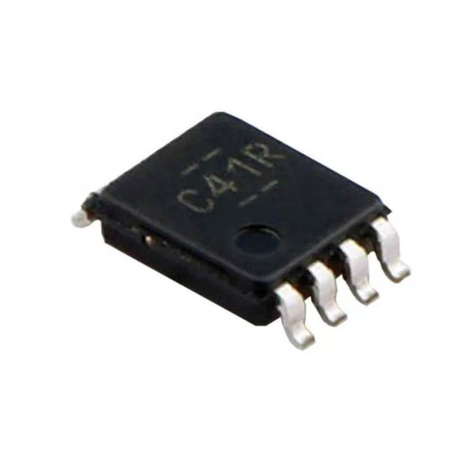




Product Overview
The SN74LVC2G241DCUR is a dual non-inverting buffer and line driver with 3-state outputs, manufactured by Texas Instruments as part of the LVC (Low-Voltage CMOS) logic family. Designed for 1.65-V to 5.5-V VCC operation, this device is organized as two independent 1-bit line drivers with separate output-enable (1OE, 2OE) control inputs, making it ideal for bus-oriented applications requiring selective signal routing. The DCU package (VSSOP-8) occupies only 2.0 x 3.1 mm of board space, enabling high-density PCB layouts. Key highlights include a maximum propagation delay of 4.1 ns at 3.3 V, ±24-mA balanced output drive at 3.3 V, over-voltage tolerant inputs up to 5.5 V, and Ioff circuitry that supports live insertion and partial-power-down operation. The device can also serve as a down-translator, converting input logic levels up to 5.5 V down to the VCC rail voltage.
Key Specifications
| Logic Family | LVC (Low-Voltage CMOS) |
| Number of Channels | 2 |
| Configuration | 2 x 1-bit non-inverting buffer/driver |
| Supply Voltage Range (VCC) | 1.65 V to 5.5 V |
| Input Voltage Range | 0 V to 5.5 V (over-voltage tolerant) |
| Propagation Delay (tpd, max) | 4.1 ns at 3.3 V |
| Output Drive Current (IOH/IOL at 3.3 V) | ±24 mA |
| Output Drive Current (IOH/IOL at 4.5 V) | ±32 mA |
| Quiescent Supply Current (ICC, max) | 10 µA |
| Output Type | 3-State |
| Input Type | Standard CMOS |
| Polarity | Non-Inverting |
| Output Enable Active Level | 1OE: Active Low; 2OE: Active High |
| VOH at IOH = -24 mA, 3.3 V | 2.4 V (min) |
| VOL at IOL = 24 mA, 3.3 V | 0.4 V (max) |
| Output Ground Bounce (VOLP, typ) | < 0.8 V at VCC = 3.3 V |
| Output VOH Undershoot (VOHV, typ) | > 2 V at VCC = 3.3 V |
| Ioff Support | Yes (live insertion / partial power-down) |
| Latch-Up Performance | > 100 mA per JESD 78, Class II |
| ESD Protection (HBM) | 2000 V (JESD 22, A114-A) |
| ESD Protection (CDM) | 1000 V (JESD 22, C101) |
| Package | VSSOP-8 (DCU), 2.0 x 3.1 mm |
| Operating Temperature Range | -40 to +125 deg C |
| RoHS / REACH | Compliant |
| MSL Rating | Level-1-260C-UNLIM |
Features
- Dual non-inverting buffer/line driver with independent 3-state output-enable controls (1OE active-low, 2OE active-high)
- Wide supply voltage range: 1.65 V to 5.5 V, supporting mixed-voltage system designs
- Over-voltage tolerant inputs accept signals up to 5.5 V independent of VCC
- Maximum propagation delay of only 4.1 ns at 3.3 V for high-speed signal buffering
- Balanced ±24-mA output drive at 3.3 V; ±32-mA output drive at 4.5 V
- Ultra-low quiescent current: 10-µA maximum ICC for power-sensitive applications
- Ioff circuitry supports live insertion, partial-power-down mode, and back-drive protection
- Down-translation capability: converts inputs up to 5.5 V down to VCC level
- Typical output ground bounce (VOLP) < 0.8 V and VOH undershoot (VOHV) > 2 V at 3.3 V
- Latch-up immunity exceeds 100 mA per JESD 78, Class II
- Available in Texas Instruments NanoFree package technology for minimum footprint
Applications
- AV receivers and home theater systems
- Blu-ray and DVD players/recorders
- Desktop and notebook PCs
- Portable media players and mobile internet devices
- GPS personal navigation devices
- Embedded PCs and digital video cameras
- Pro audio mixers and network projector front-ends
- Memory address drivers, clock drivers, and bus-oriented receivers/transmitters
 English
  简体中文
简体中文  Español
  العربية