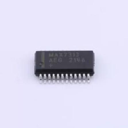
The MAX7313AEG+T operates as an I2C-addressable 16-port I/O expander with integrated PWM LED current control, combining GPIO expansion and LED driving in a single device.
I2C Interface and Addressing: The device communicates via a standard I2C/SMBus interface at up to 400 kbps. The 7-bit slave address is determined by the AD0, AD1, and AD2 pins, each of which can be connected to one of four states (GND, V+, SCL, SDA), yielding 64 unique addresses. This allows up to 64 MAX7313 devices on one I2C bus. The host writes to configuration, output, PWM, and blink registers, and reads from input, interrupt, and status registers using standard I2C read/write protocols.
I/O Port Configuration: Each of the 16 ports (P0-P15) is individually configurable through an 8-bit configuration register pair (one for P0-P7, one for P8-P15). When configured as an output, the port acts as an open-drain current sink capable of sinking up to 50 mA at up to 5.5V. When configured as an input, the port has transition detection circuitry that monitors for logic level changes. The input threshold is referenced to V+, and inputs are overvoltage protected to 5.5V, allowing direct connection to 5V logic systems even when V+ is as low as 2V.
PWM Current Control Architecture: The 8-bit PWM current control uses a hierarchical scheme. The 4-bit global intensity register (O0-O3) sets a coarse current level applied to all outputs simultaneously. This provides 14 effective intensity steps (fully off is step 0, then 14 steps from minimum to fully on). The 4-bit individual intensity register for each output (I0-I3) then divides the globally set current into 16 finer steps. The effective duty cycle for each output is proportional to (Global + 1) x (Individual + 1) / (16 x 16), giving up to 224 unique intensity levels. The PWM frequency is derived from an internal oscillator and is typically 1.5 kHz, fast enough to avoid visible flicker in LED applications.
Alternatively, the PWM control can be switched to a unified 8-bit mode where a single 8-bit register sets all outputs to the same intensity, useful for applications like uniform backlight dimming.
Two-Phase Blink Engine: Each output has two blink phase bits (Phase 0 and Phase 1). During Phase 0, the output can be set to on, off, or blink; during Phase 1, independently. All outputs share the same blink timing (controlled by the blink period register), but each output independently selects its behavior in each phase. The two-phase architecture enables grouping LEDs into synchronized blink patterns: for example, Phase 0 could have the red LEDs on and green LEDs off, while Phase 1 has the reverse, creating an alternating pattern without any host CPU overhead.
Transition Detection and Interrupt: When any input-configured port detects a logic level transition (rising or falling edge), the transition is latched in the transition detect register. The INT output (active-low, open-drain) asserts when any transition is detected, providing an interrupt to the host processor. The host reads the transition detect register to identify which port(s) changed, then clears the interrupt by reading the register. This eliminates the need for polling and reduces host CPU overhead.
Hot-Insertion Protection: During power-down (V+ = 0V), an internal circuit monitors V+ and holds all I/O pins, SDA, SCL, INT, and AD0-AD2 in a high-impedance state. This prevents parasitic conduction paths that could damage the device or corrupt the I2C bus when a card containing the MAX7313 is inserted into a powered system. The inputs can withstand up to 6V in this state, exceeding the 5.5V operating range.
Standby Mode: When all outputs are off and no I2C communication is occurring, the device enters a low-power standby state drawing only 1.2 µA (typical). The I2C interface remains active and can wake the device on address match. The transition detection circuit also remains active in standby, allowing interrupt-driven input monitoring at near-zero power.





 English
  简体中文
简体中文  Español
  العربية