Home > Integrated Circuits ICs > LMZ31707RVQR

LMZ31707RVQR


7A buck power module, 2.95-17Vin, 0.6-5.5Vout, 200k-1.2MHz, 95% eff, integrated inductor, B3QFN-42, -40~85C

5000

Effective Inventory
Go to Inquiry

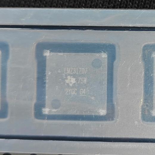
Image for reference only

Manufacturer Part:

LMZ31707RVQR

Package:

B3QFN-42 (RVQ) (10 x 10 x 4.3 mm, 0.5mm pitch)

Brand:
Product Categories:
Other recommendations you may be interested in.
Description

The LMZ31707RVQR from Texas Instruments is a SIMPLE SWITCHER 7-A step-down power module in a 10 x 10 x 4.3 mm B3QFN-42 package with tape and reel packaging. Key specifications: input voltage range 2.95 V to 17 V (with split rail, or 4.5-17 V single rail); adjustable output voltage 0.6 V to 5.5 V with 1 percent reference accuracy; maximum output current 7 A; adjustable switching frequency 200 kHz to 1.2 MHz via external resistor; efficiency up to 95 percent; integrated shielded inductor and power MOSFETs; Eco-mode light load efficiency (LLE); supports parallel operation for current sharing; split power rail option (PVIN can be lower than VIN down to 2.95 V); output voltage tracking and sequencing via SS/TR pin; power good (PWRGD) output; programmable UVLO via INH/UVLO pin; 180 degree out-of-phase SYNC_OUT clock output; synchronization to external clock via RT/CLK pin; pre-bias output startup; remote sense via SENSE+ pin; overcurrent and overtemperature protection; thermal impedance 13.3 degrees C/W; meets EN55022 Class B emissions; operating temperature -40 to +85 degrees C. Pin-compatible with LMZ31710 (10 A) and LMZ31704 (4 A). RoHS exempt. Active product status.

The LMZ31707RVQR from Texas Instruments is a SIMPLE SWITCHER power module that integrates a 7-A DC-DC buck converter with power MOSFETs, a shielded inductor, and passive components into a compact 10 x 10 x 4.3 mm QFN package. It requires as few as three external components (input capacitor, output capacitor, and voltage set resistor) to implement a complete point-of-load (POL) power supply, eliminating the loop compensation and magnetics selection process that is typically the most time-consuming part of power supply design.

The LMZ31707 is part of a pin-compatible family that includes the LMZ31704 (4 A) and LMZ31710 (10 A), allowing designers to scale current capacity without changing the PCB layout. This scalability is particularly valuable in product families where different variants require different power levels.

The input voltage range of 2.95 V to 17 V (with split rail) or 4.5 V to 17 V (single rail) covers the most common intermediate bus voltages: 3.3 V, 5 V, 12 V, and 15 V. The split rail option allows PVIN to be connected to a lower voltage (e.g., 3.3 V or 5 V) while VIN powers the control circuitry from a higher voltage, improving efficiency in applications where a low-voltage high-current rail is available.

The adjustable output voltage range of 0.6 V to 5.5 V covers all common digital and analog supply voltages: 0.9 V (FPGA core), 1.0 V, 1.2 V, 1.5 V, 1.8 V, 2.5 V, 3.3 V, 5.0 V. The 1 percent reference accuracy ensures tight voltage regulation for sensitive loads such as FPGAs, DSPs, and processors.

The switching frequency is adjustable from 200 kHz to 1.2 MHz via a single external resistor, allowing the designer to trade off efficiency (lower frequency) against solution size (higher frequency). At 1.2 MHz, the output filter uses smaller capacitors and the inductor is integrated, resulting in a very compact overall solution.

The parallel operation capability allows two or more LMZ31707 modules to share the load current through the ISHARE pin. This enables 14 A, 21 A, or higher output current configurations using the same device, with the ISHARE pin automatically balancing the current between modules.

The integrated shielded inductor eliminates the EMI concerns associated with external inductors and reduces the radiated emissions to levels that meet EN55022 Class B without additional shielding. The thermal impedance of 13.3 degrees C/W (junction to ambient) is achieved through the exposed thermal pad on the bottom of the QFN package, which must be soldered to the PCB ground plane for heat dissipation.

The LMZ31707 includes comprehensive protection features: overcurrent protection (OCP) with hiccup mode, overtemperature protection (OTP) at 175 degrees C with 10 degree hysteresis, programmable UVLO, and pre-bias startup capability that prevents the output from discharging a pre-existing voltage during startup.

At $7.21 per unit in volume (1000+), the LMZ31707RVQR is a premium power module. However, when considering the total cost of ownership (eliminating the inductor, reducing design time, smaller PCB area, fewer components, and guaranteed EMI compliance), it can be more cost-effective than a discrete implementation for many applications.

The LMZ31707RVQR operates as a synchronous buck (step-down) DC-DC converter with integrated power MOSFETs and shielded inductor, implementing current-mode control for fast transient response and easy loop compensation.

Synchronous Buck Topology: The converter uses a high-side N-channel MOSFET (control FET) and a low-side N-channel MOSFET (synchronous FET) in a synchronous buck configuration. The high-side MOSFET connects the input voltage (PVIN) to the inductor, and the low-side MOSFET provides a low-resistance current path during the off-time (replacing the Schottky diode in an asynchronous buck). This synchronous rectification eliminates the diode forward voltage drop during the off-time, significantly improving efficiency at low output voltages.

Integrated Shielded Inductor: The power inductor is integrated into the QFN package, connecting the PH (phase) node to the VOUT pin internally. The inductor is magnetically shielded to minimize radiated EMI and prevent coupling with nearby components. The inductor value is optimized for the 7 A current rating and the adjustable switching frequency range. The integration eliminates the need for the designer to select and qualify an external inductor.

Current-Mode Control: The LMZ31707 uses peak current-mode control, where the error amplifier output (VADJ voltage) sets the peak inductor current threshold. The control loop regulates the output voltage by adjusting the peak current on a cycle-by-cycle basis. Current-mode control provides inherent cycle-by-cycle current limiting, faster transient response than voltage-mode control, and easier loop compensation (single-pole response). The internal loop compensation is optimized for the integrated inductor and typical output capacitor values.

Voltage Setting: The output voltage is set by a single external resistor (RADJ) connected between the VADJ pin and AGND. The internal reference voltage is 0.6 V, and the output voltage is determined by the formula VOUT = 0.6 V x (1 + RADJ/RINT), where RINT is an internal resistor. Alternatively, the output voltage can be calculated from the lookup table in the datasheet that maps RADJ values to output voltages.

Switching Frequency and Synchronization: The switching frequency is set by an external resistor (RSET) connected from the RT/CLK pin to AGND. The frequency range is 200 kHz to 1.2 MHz. An external clock can be applied to the RT/CLK pin to synchronize the switching frequency, which is useful for avoiding beat frequencies in multi-converter systems. The SYNC_OUT pin provides a 180-degree out-of-phase clock signal that can drive another LMZ31707, reducing input ripple current in parallel or multi-rail configurations.

Parallel Current Sharing: Multiple LMZ31707 modules can be connected in parallel through the ISHARE pin. The ISHARE pin carries a current proportional to the load current of each module. When modules are connected in parallel, the ISHARE pins are tied together, and the internal control loop adjusts each module’s output voltage slightly to equalize the load current. The current sharing accuracy is typically within 10 percent between modules.

Split Rail Operation: The LMZ31707 supports separate VIN and PVIN connections. VIN powers the internal control circuitry (4.5 V minimum), while PVIN powers the output stage (2.95 V minimum). This allows the output stage to operate from a lower voltage rail (e.g., 3.3 V or 5 V) for higher efficiency at low output voltages, while the control circuitry is powered from a higher voltage (e.g., 12 V) for reliable operation.

Protection Mechanisms: Overcurrent protection (OCP) limits the peak inductor current on a cycle-by-cycle basis. If the current exceeds the OCP threshold for multiple consecutive cycles, the device enters hiccup mode (turns off and retries periodically) to prevent overheating. Overtemperature protection (OTP) shuts down the device at 175 degrees C junction temperature and restarts at 165 degrees C. The UVLO function holds the device off until the input voltage exceeds the programmed threshold.

Pin Name Type Description
A1-A4, B1-B4, C1-C4, D1-D4 PGND Power Ground Power ground connections for the output stage; low-inductance return path for the low-side MOSFET current; connect to PCB ground plane with multiple vias; these pins carry high pulsed current and must have low-impedance connections; all PGND pins are internally connected
E1, E2, F1, F2 VIN Power Input Control circuitry power supply input; minimum 4.5 V for proper operation; bypass with 1 uF ceramic capacitor to PGND; if VIN and PVIN are not connected together, VIN must be at least 4.5 V while PVIN can be as low as 2.95 V
E3, E4, F3, F4 PVIN Power Input Output stage power supply input; 2.95 V to 17 V (with VIN at 4.5 V minimum); bypass with 22 uF ceramic capacitor per the datasheet recommendations; can be connected to VIN for single-rail operation; connecting PVIN to a lower voltage rail improves efficiency at low output voltages
G1-G4, H1-H4, J1-J4 VOUT Power Output Regulated output voltage; 0.6 V to 5.5 V adjustable; up to 7 A continuous output current; connect to output capacitor bank and load; the integrated inductor connects PH to VOUT internally; remote sense connection (SENSE+) should be connected at the load point for best regulation
K1 SENSE+ Analog Input Remote sense positive input; connects to VOUT at the load point to compensate for PCB trace resistance; maximum sense voltage drop 300 mV; if remote sensing is not used, connect SENSE+ directly to VOUT at the module pins; do not leave floating
K2 VADJ Analog Input Output voltage adjustment pin; connect an external resistor (RADJ) from VADJ to AGND to set the output voltage; the internal reference is 0.6 V; the datasheet provides a resistor lookup table for common output voltages; do not apply external voltage to this pin
K3 SS/TR Analog I/O Slow start and tracking pin; an external capacitor from SS/TR to AGND sets the startup ramp time (approximately 1 ms per 10 nF); can also be used for output voltage tracking by connecting to an external tracking voltage; if not used, leave unconnected for default internal slow start
K4 PWRGD Output Power good open-drain output; pulls low when the output voltage is below the regulation threshold (typically 90 percent of set point); requires external pull-up resistor (10-100 kOhm); can be used to enable downstream loads or signal the system that power is stable; remains low during UVLO, OCP, and OTP
L1 INH/UVLO Input Inhibit and programmable UVLO pin; pulling this pin below 1.18 V disables the device; an external resistor divider from VIN can set a higher UVLO threshold; if not used, connect to VIN through a 100 kOhm resistor for automatic startup; internal pull-up enables the device when the pin is floating
L2 RT/CLK Analog Input Switching frequency set resistor and external clock input; connect a resistor (RSET) from RT/CLK to AGND to set the switching frequency (200 kHz to 1.2 MHz); alternatively, apply an external clock signal to synchronize the switching frequency; the device automatically detects whether a resistor or clock is connected
L3 SYNC_OUT Output 180-degree out-of-phase clock output; provides a clock signal at the switching frequency shifted by 180 degrees; used to synchronize a second LMZ31707 module for input ripple cancellation; can drive up to 3 additional modules; leave unconnected if not used
L4 ISHARE Analog I/O Current share pin for parallel operation; carries a current proportional to the output current; connect ISHARE pins of all parallel modules together; the internal control loop adjusts each module to share current equally; leave unconnected for single-module operation
M1-M4 AGND Analog Ground Analog ground for the control circuitry; keep separate from PGND on the PCB and connect at a single point near the module; bypass capacitors for VADJ, SS/TR, and RT/CLK connect to AGND; quiet reference point for the error amplifier
Application Description
FPGA/Processor Core Power Provide 0.9-1.2 V core voltage at up to 7 A from 5 V or 12 V intermediate bus; 1 percent output accuracy ensures reliable FPGA operation; fast transient response handles sudden core current changes; PWRGD signals FPGA when core voltage is stable; parallel two modules for 14 A core current; tracking ensures proper power-up sequencing with I/O voltage
Telecom POL Converter Convert 12 V bus to 3.3 V, 2.5 V, 1.8 V, or 1.2 V at up to 7 A for telecom line cards and base station equipment; EN55022 Class B compliance eliminates EMI concerns; parallel operation supports higher current loads; SYNC_OUT reduces input ripple in multi-rail systems; -40 to 85 C operating range suits telecom environments
Test and Measurement Power DSP, ADC, and FPGA devices in automated test equipment; 0.6-5.5 V output range covers all common digital and analog supply voltages; low output ripple and noise for sensitive analog circuits; remote sense compensates for long PCB traces; programmable UVLO ensures orderly power-up
Medical Equipment Power Provide isolated and regulated power rails for medical imaging and diagnostic equipment; 7 A output handles high-performance processors and FPGAs; overcurrent and overtemperature protection ensures safe operation; pre-bias startup prevents discharge of backup batteries; compact 10×10 mm footprint saves space in dense medical enclosures
Embedded Computing Power ARM processors, SoCs, and memory in embedded computing modules (COM Express, QSeven); adjustable output voltage via resistor simplifies BOM for different voltage rails; parallel operation provides 14 A for high-performance processors; Eco-mode reduces power consumption during idle periods
Model Manufacturer Compatibility Key Difference
LMZ31704RVQR TI Pin-Compatible, Lower Current 4 A version of the same power module family; pin-compatible with LMZ31707 in B3QFN-42; same input/output voltage range; same features (parallel, sync, tracking); use when 4 A is sufficient for lower cost; same 10x10x4.3 mm package
LMZ31710RVQR TI Pin-Compatible, Higher Current 10 A version of the same power module family; pin-compatible with LMZ31707 in B3QFN-42; same input/output voltage range; higher current for more demanding loads; use when 7 A is insufficient; same package footprint
TPSM84209 TI Similar Module, Different Package 9 A power module in a 5 x 5.5 x 4 mm QFN package; smaller footprint than LMZ31707; input 4.5-28 V; output 0.9-5.5 V; similar integrated inductor concept; not pin-compatible; use when a smaller module size is needed and higher input voltage is required
VXO7803-1000 CUI Inc Alternative Power Module 3 A 10x10x4 mm power module; lower current; input 4.5-36 V; output 3.3 V fixed; much wider input range; lower cost; not pin-compatible; use for higher input voltage applications with lower current requirements
ISL8240M Renesas Alternative Dual Module Dual 4 A (8 A total) buck power module in 15x15x5.3 mm QFN; two independent outputs; input 2.7-6 V; lower input voltage range; higher current density; not pin-compatible; use for dual-rail low-voltage applications
Recommend Parts
PMIC for AM335x, 3 bucks, 2 LDOs, battery charger, WLED, I2C, VQFN-48

Brand:

Package:

VQFN-48 (6×6 mm, 0.4 mm pitch)
In stock:
8909pcs

Cargo cycle: 3~7 Days
The minimum order is 1

Go to Inquiry
Octal D-type flip-flop, edge-triggered, async clear, 28MHz, SOP-20

Brand:

Package:

SOP-20 (NS) (12.6×7.8 mm)
In stock:
8359pcs

Cargo cycle: 3~7 Days
The minimum order is 1

Go to Inquiry
3-to-8 decoder/demux, active-low outputs, 3 enable inputs, 15ns, PDIP-16

Brand:

Package:

PDIP-16 (24.33×9.4 mm, Through-Hole)
In stock:
11952pcs

Cargo cycle: 3~7 Days
The minimum order is 1

Go to Inquiry
2W mono Class-AB audio amp, BTL speaker + SE headphone, 2.5-5.5V, HVSSOP-8

Brand:

Package:

HVSSOP-8 (DGN) (3.0×4.9 mm, PowerPAD)
In stock:
3337pcs

Cargo cycle: 3~7 Days
The minimum order is 1

Go to Inquiry
10/100 Ethernet PHY, MII/RMII/SNI, Auto-MDIX, 270mW, LQFP-48, commercial

Brand:

Package:

LQFP-48 (7×7 mm)
In stock:
14754pcs

Cargo cycle: 3~7 Days
The minimum order is 1

Go to Inquiry
Octal bus transceiver, 3-state outputs, 2-6V, 12ns tpd, TSSOP-20

Brand:

Package:

TSSOP-20 (6.5×6.4 mm)
In stock:
2638pcs

Cargo cycle: 3~7 Days
The minimum order is 1

Go to Inquiry
Quality Assurance

All electronic components we source from our partnered supply chains go through strict incoming inspections.Through careful testing, we ensure everything delivered to customers is genuine original parts and meets quality requirements.In addition, we keep complete inspection records to make the entire supply chain process clear and traceable.

Certification
We have obtained a number of professional certifications and built our own professional testing laboratory.This ensures that every product we deliver to our customers meets the highest quality requirements.We conduct tests in strict accordance with procedures to ensure stable product quality and accurate parameters.To guarantee genuine original parts, we also cooperate with reliable third-party testing institutions for strict quality inspection.We always attach great importance to quality and fully comply with industry standards, relevant regulations, and ISO 9001:2015 requirements.

Shipping & Payment

All electronic components we source from our partnered supply chains go through strict incoming inspections.Through careful testing, we ensure everything delivered to customers is genuine original parts and meets quality requirements.In addition, we keep complete inspection records to make the entire supply chain process clear and traceable.

Certification
We have obtained a number of professional certifications and built our own professional testing laboratory.This ensures that every product we deliver to our customers meets the highest quality requirements.We conduct tests in strict accordance with procedures to ensure stable product quality and accurate parameters.To guarantee genuine original parts, we also cooperate with reliable third-party testing institutions for strict quality inspection.We always attach great importance to quality and fully comply with industry standards, relevant regulations, and ISO 9001:2015 requirements.

Service & Packaging

All electronic components we source from our partnered supply chains go through strict incoming inspections.Through careful testing, we ensure everything delivered to customers is genuine original parts and meets quality requirements.In addition, we keep complete inspection records to make the entire supply chain process clear and traceable.

Certification
We have obtained a number of professional certifications and built our own professional testing laboratory.This ensures that every product we deliver to our customers meets the highest quality requirements.We conduct tests in strict accordance with procedures to ensure stable product quality and accurate parameters.To guarantee genuine original parts, we also cooperate with reliable third-party testing institutions for strict quality inspection.We always attach great importance to quality and fully comply with industry standards, relevant regulations, and ISO 9001:2015 requirements.



