TLP291GB-TP.SE


1-ch phototransistor optocoupler, CTR 100-400% (GB rank), 3750Vrms isolation, SOP-4, -55~110C, NRND

153100

Effective Inventory
Go to Inquiry

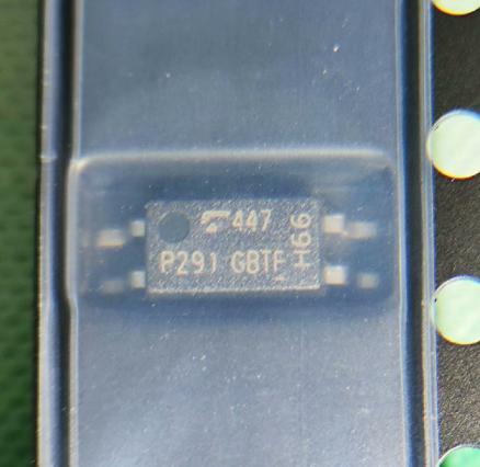
Image for reference only

Manufacturer Part:

TLP291GB-TP.SE

Package:

SOP-4 / SO4 (2.6 x 7.0 x 2.1 mm), 11-3C1

Brand:
Other recommendations you may be interested in.
Description

The TLP291GB-TP.SE from Toshiba is a single-channel phototransistor output optocoupler in a compact SOP-4 (SO4) package (2.6 x 7.0 x 2.1 mm). It consists of a gallium arsenide infrared emitting diode optically coupled to a phototransistor, providing 3750 Vrms minimum isolation voltage. The GB rank specifies a current transfer ratio (CTR) of 100% to 400% at IF=5mA, VCE=5V. Key specifications: collector-emitter voltage 80V, forward current 50mA, collector current 50mA, VCE(sat) 0.3V max, reverse voltage 5V, total power dissipation 200mW. Switching characteristics: typical rise time 2-4us, fall time 3-7us. Operating temperature: -55 to 110C. Safety approvals: UL 1577, cUL, EN 60747-5-5 (VDE), EN IEC 62368-1 (VDE), GB 4943.1-2022 (CQC). Creepage/clearance: 5.0mm minimum. The TP suffix denotes tape and reel packaging (2500 units/reel), SE suffix denotes enhanced version. Status: Not Recommended for New Designs (Toshiba recommends TLP291(SE or TLP293 as replacements). RoHS compliant.

The TLP291GB-TP.SE from Toshiba is a single-channel phototransistor output optocoupler housed in an ultra-thin SOP-4 (SO4) package measuring just 2.6 x 7.0 x 2.1 mm. The device consists of a gallium arsenide (GaAs) infrared emitting diode (IRED) optically coupled to a silicon NPN phototransistor, providing galvanic isolation between input and output circuits.

The GB rank designation specifies a current transfer ratio (CTR) range of 100% to 400% at IF=5mA and VCE=5V at 25C, meaning the phototransistor collector current equals 1x to 4x the LED forward current. This relatively high CTR range makes the GB rank suitable for low-current drive applications where the input LED current budget is limited, such as microcontroller GPIO-driven isolation circuits.

Key electrical specifications include: collector-emitter breakdown voltage (VCEO) of 80V minimum, forward current rating of 50mA maximum, collector current rating of 50mA maximum, collector-emitter saturation voltage (VCE(sat)) of 0.3V maximum at IC=2.4mA, IF=8mA, and total package power dissipation of 200mW. The input LED forward voltage is typically 1.25V at IF=5mA, with a maximum reverse voltage rating of 5V.

The device provides 3750 Vrms minimum isolation voltage (tested for 1 minute), making it suitable for reinforced insulation applications in power supplies, programmable logic controllers (PLCs), and communication interfaces. The creepage distance and clearance are both 5.0mm minimum, with insulation thickness of 0.4mm minimum, meeting the construction requirements for safety-certified optocouplers.

Switching characteristics include typical rise time of 2us and fall time of 3us (at VCC=10V, IC=2mA, RL=100 ohm), with turn-on time of 3us and turn-off time of 3us typical. These moderate switching speeds make the device suitable for signal isolation rather than high-speed data communication.

The TLP291GB-TP.SE carries comprehensive safety approvals: UL 1577 (File No. E67349), cUL (CSA Component Acceptance Service No. 5A), EN 60747-5-5 (VDE), EN IEC 62368-1 (VDE), and GB 4943.1-2022 (CQC). The VDE option (V4 suffix) provides additional certification with maximum operating insulation voltage of 707 Vpk and highest permissible overvoltage of 6000 Vpk.

The TP suffix indicates tape and reel packaging with 2500 units per reel, suitable for automated SMT assembly. The SE suffix denotes the enhanced version with improved switching characteristics. Note: Toshiba marks the TLP291 as Not Recommended for New Designs and recommends TLP291(SE or TLP293 as replacement products for new designs. The device operates over a wide temperature range of -55C to 110C and is RoHS compliant.

The TLP291GB-TP.SE operates as a phototransistor output optocoupler, converting electrical input signals to optical signals and back to electrical signals to achieve galvanic isolation between circuits.

Input Stage (LED): The input side consists of a gallium arsenide (GaAs) infrared emitting diode (IRED). When forward current (IF) flows through the LED, it emits infrared radiation at a wavelength of approximately 940nm. The forward voltage drop across the LED is typically 1.25V at IF=5mA. The LED must be driven with a current-limiting resistor calculated from the driving voltage: R = (VDRIVE – VF) / IF, where VF is the LED forward voltage. Typical drive currents range from 1mA to 20mA for signal isolation applications.

Optical Coupling: The infrared light from the LED propagates across a transparent dielectric insulation layer within the package. This insulation layer provides the galvanic isolation barrier with a minimum thickness of 0.4mm, achieving 3750 Vrms isolation voltage. The optical coupling efficiency between the LED and phototransistor determines the current transfer ratio (CTR). For the GB rank, the CTR ranges from 100% to 400% at the specified test conditions, meaning IC = CTR x IF.

Output Stage (Phototransistor): The output side consists of a silicon NPN phototransistor. When infrared photons from the LED strike the phototransistor base-collector junction, they generate electron-hole pairs (photocurrent) in the base region. This photocurrent acts as the base drive for the NPN transistor, causing a larger collector current to flow. The phototransistor provides both photodetection and current amplification in a single device, which is why CTR can exceed 100% — the phototransistor current gain (hFE) amplifies the initial photocurrent.

CTR Behavior: The CTR is not constant and varies with: (1) Forward current IF — CTR typically peaks at IF=5-10mA and decreases at both lower and higher currents; (2) Temperature — CTR decreases at temperatures above 25C due to reduced LED efficiency and phototransistor gain; (3) Age — CTR degrades over time due to LED output degradation, typically 10-20% over 10 years at rated current. Design margins must account for these variations, especially when using the GB rank 100% minimum CTR.

Switching Behavior: The phototransistor switching speed is limited by its relatively large junction area (needed for high photosensitivity) and charge storage effects. Rise time (tr) and fall time (tf) are typically 2-4us and 3-7us respectively. The turn-off is slower than turn-on because the phototransistor must clear stored base charge without a dedicated base pull-down resistor. For faster switching, a base-emitter resistor can be added, or a faster optocoupler architecture (e.g., photodiode + amplifier) should be selected.

Isolation: The galvanic isolation is achieved by the physical separation between the LED and phototransistor chips, with only optical coupling bridging the gap. The isolation barrier withstands 3750 Vrms for 1 minute and provides continuous isolation at working voltages up to the rated insulation voltage. The parasitic capacitance across the isolation barrier (typically 0.5-1pF) limits common-mode transient immunity, while the isolation resistance exceeds 10^12 ohms.

Pin Name Type Description
1 ANODE Input LED anode; connect to positive side of drive circuit through current-limiting resistor; forward current IF up to 50mA; forward voltage VF typically 1.25V at IF=5mA
2 CATHODE Input LED cathode; connect to ground or negative side of drive circuit; reverse voltage must not exceed 5V
3 EMITTER Output Phototransistor emitter; connect to output circuit ground or reference; collector current IC flows from collector (Pin 4) through the load to emitter
4 COLLECTOR Output Phototransistor collector; connect through pull-up resistor to output supply voltage; VCEO maximum 80V; VCE(sat) maximum 0.3V at IC=2.4mA, IF=8mA
Application Description
Switching Power Supply Feedback Isolates the secondary-side error amplifier output from the primary-side PWM controller in isolated flyback/forward converters; CTR range 100-400% provides adequate loop gain; 3750Vrms isolation meets safety requirements for mains-powered supplies
PLC Digital I/O Isolation Isolates PLC digital input/output channels from field wiring; wide -55 to 110C temperature range suits industrial environments; VDE and UL approvals meet machinery safety standards
Communication Interface Isolation Provides galvanic isolation for RS-232, RS-485, CAN, and other communication interfaces; prevents ground loops between interconnected equipment; 5mm creepage/clearance meets industrial spacing requirements
Microcontroller Signal Isolation Isolates MCU GPIO signals from high-voltage or noisy circuits; GB rank CTR (100-400%) allows direct MCU pin drive at 5-10mA IF; simple 4-pin interface minimizes component count
Gate Drive Signal Isolation Low-frequency IGBT/MOSFET gate drive isolation for motor drives and inverters; 80V VCEO provides margin for gate drive voltage levels; switching speed suitable for PWM frequencies up to approximately 100kHz
Model Manufacturer Compatibility Key Difference
TLP291(SE Toshiba Recommended Replacement Same package and pinout; enhanced switching speed; SE version with improved performance; Toshiba recommended replacement for new designs
TLP293 Toshiba Recommended Replacement Same package size; different switching speed; Toshiba recommended replacement for new designs; check CTR rank availability
PC817C Sharp/IXYS Functionally Similar DIP-4 package (not SOP-4); CTR 200-400% (C rank); 5000Vrms isolation; through-hole mounting; different footprint
EL817C Everlight Functionally Similar DIP-4 package; CTR 200-400%; 5000Vrms isolation; industry-standard PC817 compatible; different package type
SFH6156-3T Vishay Functionally Similar SOP-4 package; CTR 100-200% (Rank 3); 5300Vrms isolation; similar low-profile design; different CTR range
Recommend Parts
Transistor output optocoupler, 5000Vrms isolation, CTR 100-200% (GRL rank), VDE approved DIP-4

Brand:

Package:

DIP-4 (4.6 x 7.62 x 3.5 mm, 7.62mm pitch)
In stock:
12686pcs

Cargo cycle: 3~7 Days
The minimum order is 1

Go to Inquiry
Quad phototransistor optocoupler, 55V, CTR 100%, 2500Vrms, 16-DIP

Brand:

Package:

16-DIP (9.82 x 7.62 x 4.2 mm)
In stock:
14066pcs

Cargo cycle: 3~7 Days
The minimum order is 1

Go to Inquiry
IGBT gate drive photocoupler, +/-2.5A peak, 3750Vrms isolation, 20kV/us CMTI, SO6 T/R

Brand:

Package:

5-pin SO6 (3.7 x 7.0 x 2.1 mm, 2.54mm pitch, gull-wing, SMD)
In stock:
1806pcs

Cargo cycle: 3~7 Days
The minimum order is 1

Go to Inquiry
100V N-ch power MOSFET, 100A/207A, 3.4mOhm RDS(on), U-MOS VIII-H, TO-220, 255W, 140nC Qg, switching regulators

Brand:

Package:

TO-220 (3-pin + Tab) (10.16 x 15.1 x 4.45 mm, 2.54mm pitch)
In stock:
596pcs

Cargo cycle: 3~7 Days
The minimum order is 1

Go to Inquiry
Quality Assurance

All electronic components we source from our partnered supply chains go through strict incoming inspections.Through careful testing, we ensure everything delivered to customers is genuine original parts and meets quality requirements.In addition, we keep complete inspection records to make the entire supply chain process clear and traceable.

Certification
We have obtained a number of professional certifications and built our own professional testing laboratory.This ensures that every product we deliver to our customers meets the highest quality requirements.We conduct tests in strict accordance with procedures to ensure stable product quality and accurate parameters.To guarantee genuine original parts, we also cooperate with reliable third-party testing institutions for strict quality inspection.We always attach great importance to quality and fully comply with industry standards, relevant regulations, and ISO 9001:2015 requirements.

Shipping & Payment

All electronic components we source from our partnered supply chains go through strict incoming inspections.Through careful testing, we ensure everything delivered to customers is genuine original parts and meets quality requirements.In addition, we keep complete inspection records to make the entire supply chain process clear and traceable.

Certification
We have obtained a number of professional certifications and built our own professional testing laboratory.This ensures that every product we deliver to our customers meets the highest quality requirements.We conduct tests in strict accordance with procedures to ensure stable product quality and accurate parameters.To guarantee genuine original parts, we also cooperate with reliable third-party testing institutions for strict quality inspection.We always attach great importance to quality and fully comply with industry standards, relevant regulations, and ISO 9001:2015 requirements.

Service & Packaging

All electronic components we source from our partnered supply chains go through strict incoming inspections.Through careful testing, we ensure everything delivered to customers is genuine original parts and meets quality requirements.In addition, we keep complete inspection records to make the entire supply chain process clear and traceable.

Certification
We have obtained a number of professional certifications and built our own professional testing laboratory.This ensures that every product we deliver to our customers meets the highest quality requirements.We conduct tests in strict accordance with procedures to ensure stable product quality and accurate parameters.To guarantee genuine original parts, we also cooperate with reliable third-party testing institutions for strict quality inspection.We always attach great importance to quality and fully comply with industry standards, relevant regulations, and ISO 9001:2015 requirements.



