
Introduction / Industry Overview
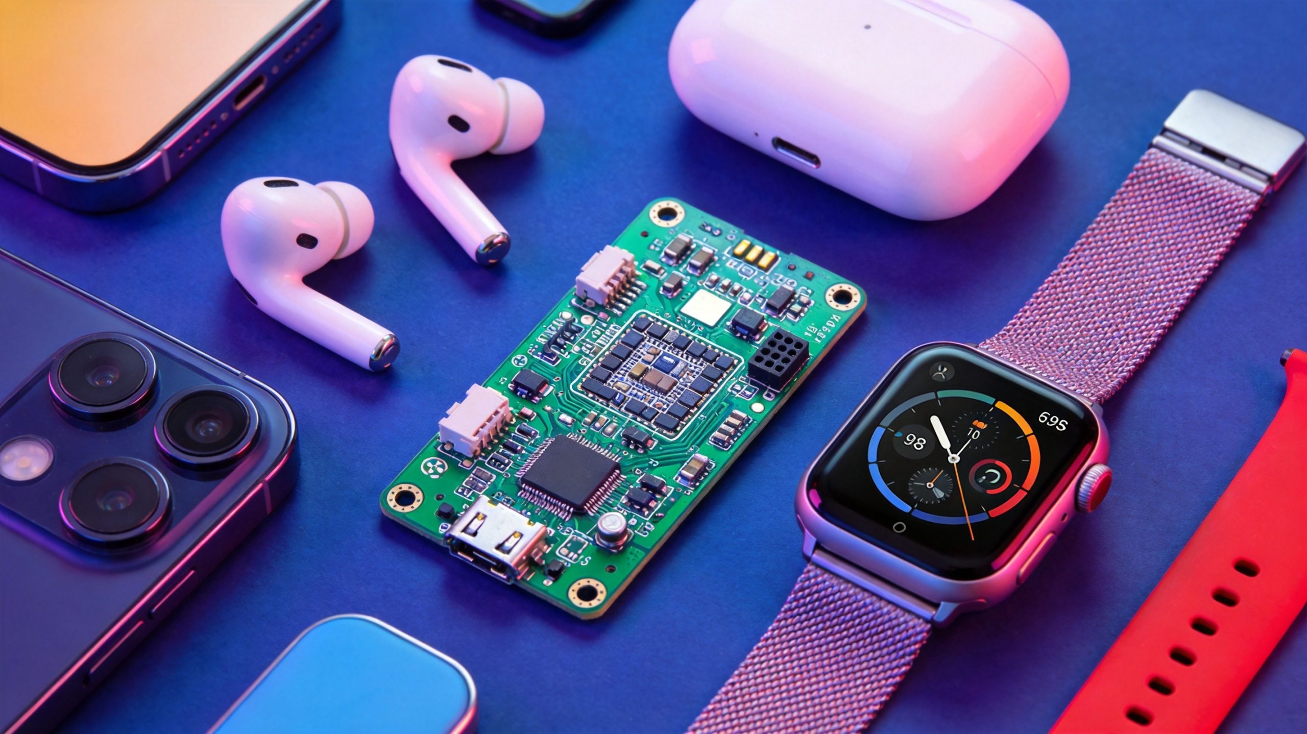
Consumer electronics is the engine room of the PCB industry. By volume, it accounts for the largest share of global PCB production—smartphones alone consumed over USD 19.5 billion in HDI PCBs in 2025, with the market projected to reach USD 34 billion by 2032 at a CAGR of 8.3% (MarketsandMarkets, 2025). The defining imperative is unambiguous: make it smaller, make it faster, and make it last longer on a battery—all while keeping costs on a relentless downward trajectory.
This imperative has driven three structural shifts in consumer electronics PCB design. First, high-density interconnect (HDI) technology has become the baseline, not the premium option—any device with a BGA-pitch IC below 0.5 mm effectively requires HDI construction. Second, rigid-flex and fully flexible PCBs have moved from niche applications (military, medical) into the consumer mainstream, driven by wearables, foldable phones, and true wireless stereo (TWS) earbuds. Third, the integration of multiple wireless protocols (Bluetooth LE, Wi-Fi 6/7, Thread, Matter, UWB) on a single board has created RF-audio-digital co-design challenges that were unheard of five years ago.
This article examines the core technologies, real-world application cases, and future trajectory of consumer electronics PCB design, with a focus on HDI miniaturization, wearable device challenges, and IoT wireless integration.
Featured Image
Core Technology Analysis
HDI Miniaturization: From 100μm Microvias to Sub-50μm Frontiers
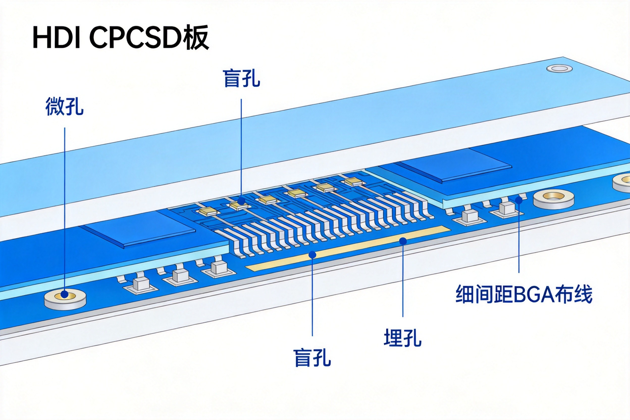
High-Density Interconnect (HDI) PCB technology is defined by IPC-2226 as boards with microvia diameters ≤150 μm, line width/spacing ≤75 μm, and via-in-pad structures supporting BGA pitches down to 0.25 mm. These specifications have been sufficient for the past decade of smartphone and tablet design. But the next generation of devices—6G modems, AI-powered wearables, foldable phones with 1 mm hinge mechanisms—is pushing HDI beyond its current limits.
Sub-50μm Microvias: Traditional UV laser drilling struggles with microvias below 50 μm due to heat-induced substrate damage. Femtosecond laser drilling (pulse duration <1 fs) ablates material without thermal effects, enabling 20–40 μm microvias in LCP and polyimide substrates—50% smaller than today’s standard, allowing 4× more interconnects per cm². FR4PCB.TECH’s R&D division reports initial yields of 98% for 30 μm microvias in LCP substrates, with low-volume production availability expected by 2026.
Nanoscale Traces via Atomic Layer Deposition (ALD): ALD deposits copper atoms one layer at a time, creating 5–10 μm wide traces with 99.999% purity. Unlike subtractive etching—which risks undercut and line-width variation—ALD produces uniform, high-conductivity traces ideal for AI processors requiring dense signal routing. Modified Semi-Additive Process (mSAP) has become the production bridge between traditional etching and ALD, consistently producing 20 μm traces with current manufacturing equipment.
The HDI vs. Standard PCB Gap:
| Parameter | HDI PCB | Standard PCB | Design Impact |
|---|---|---|---|
| Via Diameter | 0.10–0.15 mm | 0.30–0.50 mm | 60–70% space savings on via footprint |
| Line/Space Width | ≤75 μm | ≥100 μm | Higher routing density per layer |
| Min BGA Pitch | 0.25–0.40 mm | ≥0.50 mm | Enables advanced chip packages |
| Equivalent Layer Count | 6–12 layers | 12–24+ layers | Reduced material and processing cost |
| Board Size (equivalent function) | 30–50% smaller | Baseline | Enables compact form factors |
| Signal Integrity @ 10 Gbps | Excellent (short via stubs) | Limited (long stubs) | Critical for high-speed interfaces |
A flagship smartphone motherboard illustrates the trend: from >100 cm² in 2010 to under 40 cm² in 2025, while integrating 1200+ interconnects through 6-layer HDI with 3rd-order blind/buried vias (0.08 mm line/space). The smartphone PCB area reduction of 60%+ over 15 years is almost entirely attributable to HDI advancement.
Rigid-Flex and Fully Flexible PCBs for Wearable Devices
Wearable devices demand PCBs that conform to the human body, survive repeated bending, and operate reliably in environments ranging from sweat-soaked workouts to daily showers. The material and design choices differ sharply between product categories:
Smartwatches use rigid-flex PCBs: the main board is 0.8 mm thick FR-4 (Tg ≥150°C) for component mounting, while flexible polyimide (PI) connection sections (bending radius ≥8 mm) route signals to the display, battery, and sensor modules. IPX7 waterproofing is achieved through an 8 μm nano-coating (PTFE or acrylic) combined with silicone sealing at interfaces. Component density reaches 100–200 components/cm²—2–3× that of traditional PCBA.
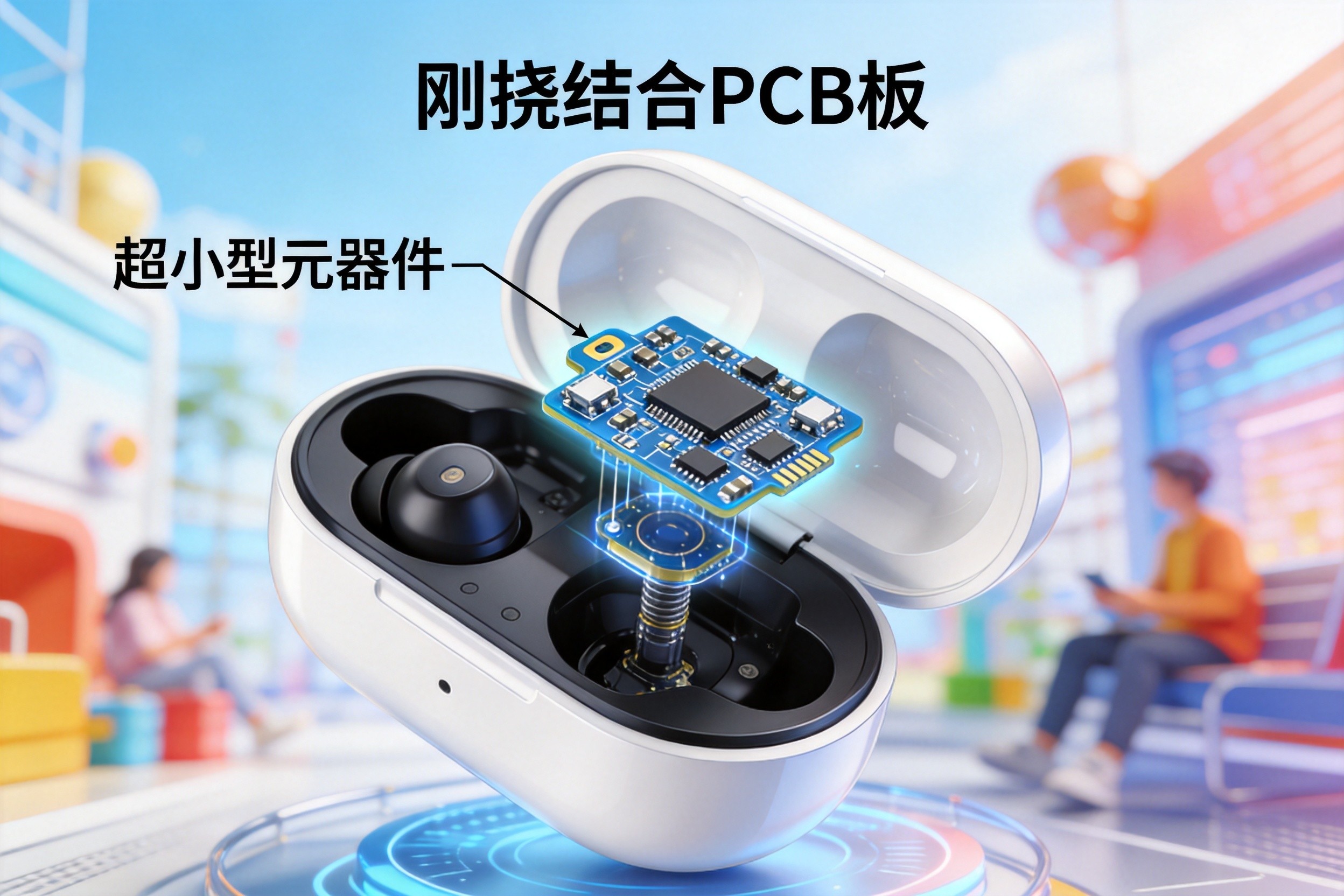
TWS Earbuds represent the extreme of miniaturization. A typical TWS PCB measures just 8 mm × 15 mm, uses 6-layer 2nd-order HDI construction with 0.08 mm blind vias, and integrates a Bluetooth SoC, ANC codec, touch controller, and battery management IC in a space smaller than a fingernail. Key design techniques include:
- Star-shaped interconnect: The Bluetooth SoC sits at the center, with FPC branches radiating to the speaker (differential audio traces, ≤3 cm), microphones (shielded, ≥0.5 mm from audio lines), battery (trace width ≥0.3 mm, copper reinforced), and touch sensors.
- Ultra-small components: 01005 (0.4 mm × 0.2 mm) and even 008004 (0.2 mm × 0.1 mm) passive components, with WLCSP-packaged ICs at 0.3 mm pitch. Placement accuracy of ±0.01 mm is required—dual-camera vision alignment systems have reduced component overlap rates from 4% to 0.1%.
- EMC management for wireless charging: The wireless charging coil operates at 110–205 kHz, and without proper shielding, radiated emissions exceed 54 dBμV/m (GB/T 17799.3 limit), causing Bluetooth 2.4 GHz interference. Solutions include star-type multi-point grounding (via diameter 0.3 mm, spacing 2 mm, ground resistance <0.5 Ω), copper foil shielding under the coil (covering 120%+ of coil area, ground resistance <0.3 Ω), and π-type filtering (10 μF X-capacitor + 0.1 μF Y-capacitor + 22 μH common-mode choke). The wireless charging PCB must be spaced ≥3 mm from the Bluetooth module—every 1 mm reduction increases radiation by 6 dBμV/m and degrades Bluetooth SNR by 8 dB.
Medical-grade wearables (continuous glucose monitors, ECG patches) require fully flexible PCBs with 0.1 mm PI substrate certified for biocompatibility per ISO 10993-5. Ultra-low-power MCUs (e.g., MSP430, STM32L0 with 0.2 μA sleep current) and Bluetooth LE chips enable 14-day battery life from coin cells. Components are arranged along the PCB edges with a minimum bending radius of ≥5 mm.
IoT Wireless Connectivity: Multi-Protocol Co-Design
The proliferation of IoT wireless protocols has created a new category of PCB design challenge: integrating multiple RF front ends—each with different frequency bands, power levels, and antenna requirements—on a single board alongside sensors, processors, and power management.
Protocol Selection and PCB Impact:
| Protocol | Frequency | Range | الطاقة | PCB Design Impact |
|---|---|---|---|---|
| BLE 5.x/6.0 | 2.4 GHz | 10–100 m | μA sleep | 50Ω controlled impedance, antenna matching network, ground plane ≥λ/4 (31 mm) from feed |
| Wi-Fi 6/7 | 2.4/5/6 GHz | 30–100 m | mA active | Multi-band antenna, TWT power management, OFDMA coexistence |
| LoRa/LoRaWAN | Sub-1 GHz | 1–20 km | μA sleep | Low-loss substrate (Rogers RO4350B, tanδ ≤0.004), π-type antenna matching (VSWR ≤1.5) |
| NB-IoT/LTE-M | Licensed bands | Nationwide | mA active | Cellular certification (FCC/CE/RED), power amplifier thermal management |
| Thread/Matter | 2.4 GHz | 30–50 m | mA active | Mesh networking, coexistence with BLE/Wi-Fi |
| UWB | 3.1–10.6 GHz | 10–30 m | mA active | Ultra-wideband antenna, precise time-of-flight layout |
Key PCB Design Rules for IoT Wireless:
-
Antenna placement: The antenna must be positioned at the PCB edge with a ground-plane clearance zone per the manufacturer’s reference design. Placing a chip antenna in the board center with surrounding copper is the single most common cause of range failure—measured range drops from 50 m to <10 m.
-
Ground plane integrity: For BLE, the ground plane must extend at least λ/4 (~31 mm at 2.4 GHz) in all directions from the antenna feed point. Slots or traces cutting through the ground plane under the RF section force return currents to detour, altering impedance and creating EMI. Use solid copper pours with via stitching every 3–5 mm in RF-critical areas.
-
Crystal oscillator isolation: A 32 MHz BLE crystal or 26 MHz Wi-Fi crystal generates harmonics that land precisely in the 2.4 GHz ISM band. Keep crystal traces under 10 mm, add a ground ring around the crystal footprint, and avoid routing digital signals nearby. Series damping resistors (22–47 Ω) on clock lines reduce harmonic radiation.
-
Power supply segregation: Use dedicated LDO regulators for RF modules, separate from noisy digital circuits. Place 1.0 μF and 0.1 μF bypass capacitors within 3 mm of the module’s VCC pins—parasitic inductance from longer traces degrades high-frequency decoupling effectiveness.
-
Pre-certified modules vs. bare SoCs: Pre-certified modules (ESP32-WROOM, nRF52840 module, Quectel cellular modules) dramatically simplify PCB design by handling antenna matching, crystal selection, and RF shielding internally. They trade higher BOM cost and larger footprint for faster time-to-market and reduced certification risk. Bare SoCs offer maximum customization and lower per-unit cost at volume but require full RF layout expertise and individual regulatory certification.
Low-Power Design: From Circuit to System
For battery-powered IoT devices, power consumption is not a specification—it is the specification. A smart water meter drawing 100 μA quiescent current drains a 5000 mAh battery in just 6 months; reducing to 0.2 μA extends battery life to over 8 years. PCB design contributes to low-power performance through several mechanisms:
-
Sleep-mode current minimization: Use MCU deep-sleep modes (STM32L0: 0.2 μA, nRF54L15: sub-μA), and ensure all peripheral circuits (sensors, voltage regulators, pull-up resistors) also enter low-power states. Pull-up/pull-down resistor values must be optimized: too low wastes current, too high slows signal transitions and makes logic levels noise-vulnerable.
-
Efficient voltage regulation: Buck converters for high-current rails (MCU, RF transmitter), LDOs for noise-sensitive circuits (sensors, ADC references), and power-path management ICs that disconnect the battery during shelf storage to prevent drain between factory and consumer.
-
Energy harvesting integration: PCBs for remote IoT nodes increasingly incorporate solar cells (10 μW–1 W), thermoelectric generators, or piezoelectric harvesters. These require MPPT (Maximum Power Point Tracking) ICs and supercapacitor/battery storage, adding power-management complexity to the PCB.
Typical Application Cases
Case 1: Flagship Smartphone Main Board — HDI Pushes the Limits
A 2026 flagship smartphone integrates a 3 nm application processor (0.25 mm BGA pitch), a 5G mmWave modem, LPDDR5X memory, and a 200 MP image signal processor on a main board measuring 38 cm²—60% smaller than the 2015 equivalent.
PCB Design Approach: 10-layer Any-Layer HDI (ELIC—Every Layer Interconnection) construction with mSAP-fabricated 25 μm/25 μm line/space and 40 μm laser microvias. The 5G mmWave antenna module uses a separate LCP (Liquid Crystal Polymer) substrate with 20 μm microvias for sub-6 GHz and mmWave signal integrity. SiP integration packages the AP, memory, and PMIC into a single module, reducing the PCB’s role to signal distribution and peripheral interfacing.
Result: Board area 38 cm² (vs. 95 cm² for equivalent functionality in 2015), with 10 Gbps signal integrity verified for USB-C 3.2 and PCIe 4.0 interfaces. Signal loss reduced by 30% through AI-optimized microvia placement and trace routing.
Case 2: TWS Earbuds — Miniaturization Meets EMC
A premium TWS earbud with hybrid ANC and spatial audio must fit its entire electronics—Bluetooth SoC (0.4 mm BGA), ANC codec, 3 microphones, speaker driver, touch sensor, and charging management—into a 4.5 cm³ earpiece cavity.
PCB Design Approach: 6-layer 2nd-order HDI rigid-flex construction (8 mm × 15 mm rigid section + 25 μm PI flex tails). 01005 passive components throughout, with WLCSP-packaged Bluetooth SoC. A “rigid-flex-rigid” three-section design separates the antenna (LCP flex in the earbud stem, +3 dB signal strength vs. PCB antenna), the main logic (FR-4 rigid section), and the battery/sensor interface (PI flex). The wireless charging PCB uses star-type multi-point grounding, copper foil shielding under the coil, and a 4 mm minimum distance from the Bluetooth module.
Result: IPX4 waterproofing with 5 μm nano-coating, 100,000+ bend cycles on flex sections, Bluetooth range of 12 m with concurrent wireless charging (SNR >80 dB), and manufacturing yield of 98% through AOI + X-ray inspection.
Case 3: Industrial IoT Sensor Node — 10-Year Battery Life
A LoRaWAN soil moisture sensor must operate unattended for 10 years on a single 5000 mAh lithium battery, transmitting once per day from an underground installation at 20 cm depth.
PCB Design Approach: 4-layer HDI (50 mm × 30 mm) using Rogers RO4350B substrate for the LoRa RF section (433 MHz, tanδ ≤0.004, 5 km range with ≤8 dB attenuation vs. 15 dB on FR-4). STM32L0 MCU (0.2 μA sleep) with Semtech SX1262 LoRa transceiver (0.5 μA sleep). π-type antenna matching network achieving VSWR ≤1.5. Energy harvesting via a 10 μW solar cell on the above-ground antenna housing, with MPPT charging to a supercapacitor buffer. Conformal coating for moisture and chemical resistance in soil contact.
Result: Average daily power consumption of 0.001 mAh, yielding 13.7 years of battery life from 5000 mAh. LoRa communication success rate of 99.2% at 5 km range. Data upload encrypted with AES-128 for security compliance.
Future Development Trends
Sub-50μm Microvias and ALD Trace Fabrication
Femtosecond laser drilling for 30–40 μm microvias is in lab testing with 98% yield; mass production is expected by 2027–2028, pending scale-up of laser throughput (current systems process ~1 board/minute; mass production needs 10+). ALD for 5–10 μm traces remains in research but promises to redefine the density ceiling for AI-chip PCBs. The 6G smartphone using 30 μm microvias and 8 μm traces could shrink its main PCB by 60% versus current 5G designs, enabling foldable devices with 1 mm-thin hinges. Timeframe: 30–40 μm microvias in low-volume production by 2026; mass production by 2028. ALD traces in niche applications by 2029–2030.
AI-Driven PCB Design and Manufacturing
Generative AI models trained on millions of HDI designs can produce optimized layouts in minutes—considering microvia placement, trace routing, thermal management, and EMI suppression simultaneously. Early results show a 30% reduction in signal loss for AI-designed 8-layer HDI layouts versus human-designed equivalents. Machine learning for real-time process control has reduced microvia void rates from 5% to below 1% in pilot production lines. The engineer’s role is shifting from manual layout to validating and refining AI-generated designs, ensuring they meet application-specific requirements. Timeframe: AI-assisted layout tools are already commercially available; fully autonomous HDI design optimization expected by 2028–2029.
SiP+PCB Convergence and Embedded Components
System-in-Package (SiP) integration—combining the processor, memory, RF front end, and PMIC into a single module—is converging with PCB design, where the board’s role shifts from component-level interconnection to module-level signal distribution and peripheral interfacing. This trend reduces PCB area by 40–50% and layer count by 30–40%, but increases the dependency on advanced packaging technologies and tight SiP-to-PCB interface tolerances (0.3 mm pitch board-to-board connectors). Embedded passive components (resistors, capacitors) within PCB inner layers are moving from aerospace/defense into consumer electronics, with prototype 4-layer boards integrating 1200 embedded components at 200 components/cm² density. Timeframe: SiP+PCB is already standard in flagship smartphones; embedded components will enter mainstream consumer products by 2028–2029.
Conclusion
Consumer electronics PCB design exists at the intersection of three converging pressures: relentless miniaturization, multi-protocol wireless integration, and ultra-low power consumption. The transition from 100 μm to sub-50 μm microvias, from rigid boards to rigid-flex hybrid constructions, and from single-protocol to multi-protocol RF co-design represents not incremental improvement but a generational shift in manufacturing capability. As AI-driven design tools accelerate layout optimization and SiP integration redefines the PCB’s functional role, the manufacturers who will lead are those investing in advanced HDI processes, RF design expertise, and the manufacturing precision to deliver sub-10 μm features at consumer-grade volumes and costs. For electronics companies navigating this transition, the PCB is no longer just a substrate—it is the primary differentiator in the race to smaller, smarter, and longer-lasting devices.
Looking for consumer electronics PCB manufacturing with HDI capabilities? Connect with our team to discuss miniaturization strategies and multi-protocol RF integration for your next product.
 English
  简体中文
简体中文  Español
  العربية