
Introduction / Industry Overview
Automotive electronics has undergone a structural transformation. Where electronics once accounted for roughly 15% of total vehicle cost, that figure has now exceeded 40% in premium electric vehicles (IEA, 2026), driven by the proliferation of advanced driver-assistance systems (ADAS), battery management systems (BMS), and domain-controller architectures. The global automotive electronics market was valued at approximately USD 280 billion in 2025 and is projected to reach USD 460 billion by 2030, growing at a CAGR of 10.4% (MarketsandMarkets, 2025).
Unlike consumer electronics, where a two-to-five-year design life is acceptable, automotive PCBs must endure 10–15 years and 200,000+ miles of service across extreme thermal cycling (−40°C to +150°C), continuous vibration (10–2000 Hz at up to 20 G), humidity, salt-spray exposure, and transient voltage spikes. A single field failure in a safety-critical system—braking, steering, or airbag deployment—can have catastrophic consequences. This reality has produced one of the most stringent standard matrices in electronic manufacturing: the AEC-Q series for component qualification, ISO 26262 for functional safety, ISO 16750 for environmental reliability, IPC Class 3 for workmanship, and IATF 16949 for quality management.
This article dissects the core technical requirements, application scenarios, and future trajectory of automotive electronics PCB design, with a focus on how the AEC-Q and ISO 26262 frameworks shape every decision from material selection to manufacturing process control.
Core Technology Analysis
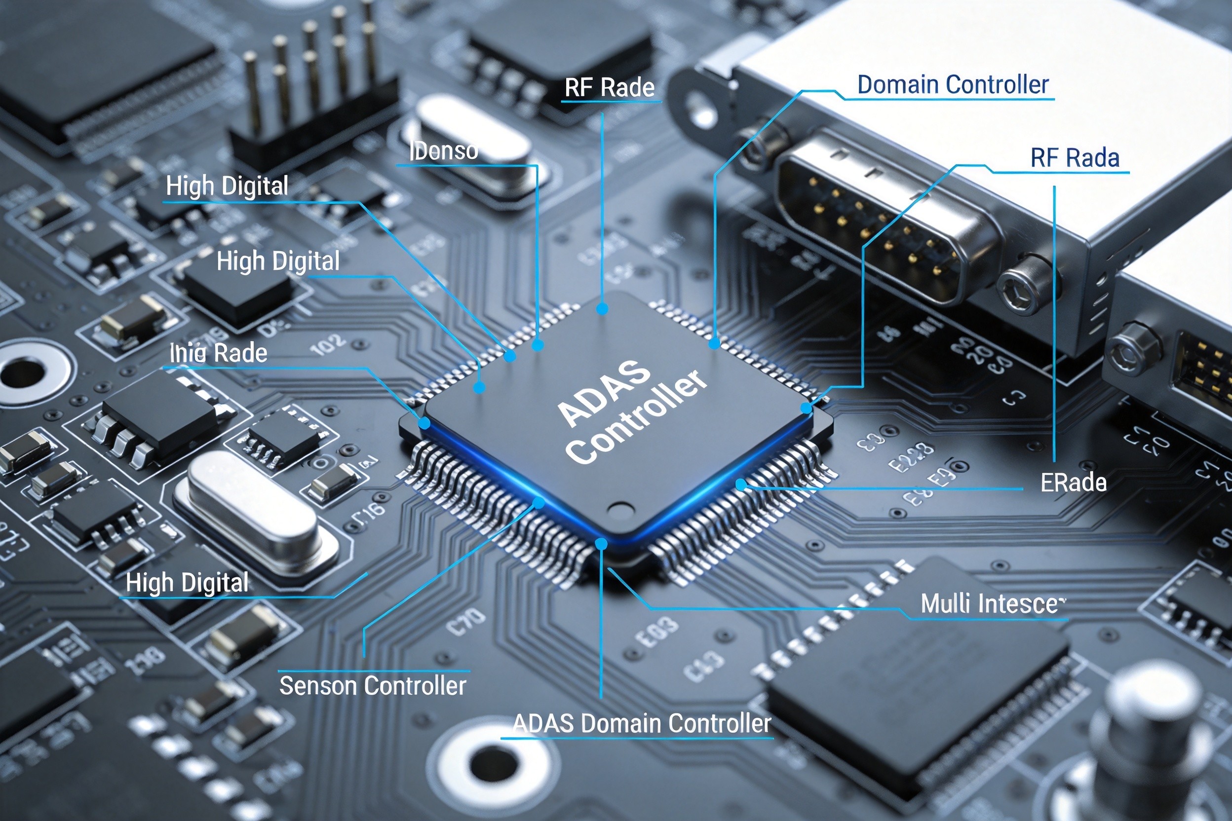
The AEC-Q Standard Matrix: Qualification from Component to Board Level
The Automotive Electronics Council (AEC) has established a family of stress-test qualification standards that form the non-negotiable baseline for any component entering the automotive supply chain:
| Standard | Scope | Key Test Conditions |
|---|---|---|
| AEC-Q100 | Integrated circuits | Temperature cycling (−40°C to +125°C, 1000+ cycles), HTOL (125°C, 1000 h), ESD (HMM 2000V+) |
| AEC-Q101 | Discrete semiconductors | Similar to Q100, with additional forward-bias stress |
| AEC-Q102 | Optoelectronics | Luminous output degradation, thermal resistance |
| AEC-Q103 | MEMS sensors | Vibration, shock, pressure cycling |
| AEC-Q104 | Multi-chip modules | Combined test protocols |
| AEC-Q200 | Passive components | Thermal cycling (−55°C to +125°C, 1000 cycles), 85°C/85% RH for 1000 h, mechanical vibration per AEC-Q200 profile |
| AEC-Q007 | Solder joint reliability (PCB level) | Thermal cycling per IPC-9701, vibration, mechanical shock |
AEC-Q007 deserves particular attention from PCB designers. Released in response to the absence of a unified board-level reliability standard—previously, each OEM defined its own requirements—AEC-Q007 is the first automotive standard that explicitly addresses solder joint reliability at the PCB level. It mandates thermal cycling tests (TCT) with failure criteria per IPC-9701, vibration testing for mechanical stress, and mechanical shock for impact resistance.
Temperature grading under AEC-Q100 defines the operational envelope:
- Grade 0: −40°C to +150°C (engine compartment, powertrain)
- Grade 1: −40°C to +125°C (general automotive, most ADAS)
- Grade 2: −40°C to +105°C (passenger compartment)
- Grade 3: −40°C to +85°C (limited applications)
The 2025 revision of AEC-Q100 (Rev H) introduced a 10-year life acceleration model, increasing the thermal cycling requirement from 1000 to 1500 cycles (−40°C ↔ +125°C, transition time <1 minute) and adding a combined “random vibration + shock” test profile—reflecting the real-world expectation of 10-year/200,000-km durability.
Material Selection: Beyond FR-4
Standard FR-4 (Tg = 130–140°C) is fundamentally inadequate for automotive applications. Its Z-axis coefficient of thermal expansion (CTE) of approximately 280 ppm/°C far exceeds copper’s 17 ppm/°C, causing plated-through-hole (PTH) copper cracking after repeated thermal cycling. AEC-Q200-compatible designs require:
- High-Tg, low-CTE laminates: Isola IS410 (Tg = 180°C, Z-CTE = 65 ppm/°C) or Rogers RO4350B (Tg = 280°C, Z-CTE = 45 ppm/°C) for high-frequency applications.
- Halogen-free certification: IEC 61249-2-21 compliance (Cl + Br < 900 ppm).
- UL 94 V-0 flame retardancy: Mandatory for all automotive PCB substrates.
The material choice has direct signal integrity implications. A documented case involved an ADAS radar board using FR-4 instead of a low-loss laminate: at 77 GHz, the FR-4’s Dk variation caused a 12° phase error in the antenna feed network, resulting in a 3.2° beam-pointing offset that violated ISO 22178 functional safety requirements. The board was redesigned with RO4350B (Dk = 3.48 ± 0.05 at 10 GHz), reducing phase error to under 2°.
Solder Joint Reliability: The ENIG Nickel Thickness Window
Automotive ECUs may undergo 3–5 rework cycles during production and service. Organic Solderability Preservative (OSP) surface finishes oxidize after multiple reflow passes, making Electroless Nickel Immersion Gold (ENIG) the industry standard for automotive PCBs. However, the nickel layer thickness must be controlled within a narrow window:
- Too thin (<2.5 μm): Insufficient barrier against copper diffusion, causing “black pad” defects and joint embrittlement.
- Too thick (>6 μm): Nickel-phosphorus alloy becomes brittle, initiating microcracks under −40°C thermal shock.
- Optimal range (3–5 μm): Test data shows 4.2 μm nickel retains >92% solder-joint shear strength after 1000 cycles of −40°C/+125°C thermal cycling, while 2.8 μm degrades to 76%.
Additionally, solder mask defined (SMD) pads are preferred over non-solder mask defined (NSMD) pads in automotive applications. SMD construction, where the solder mask overlaps the pad edge, creates a stress buffer zone that extends thermal fatigue crack initiation life by a factor of 2.3× per JEDEC JESD22-A104 testing.
ISO 26262 Functional Safety: From ASIL to PCB Layout
ISO 26262 defines Automotive Safety Integrity Levels (ASIL A through ASIL D) based on severity, exposure probability, and controllability of potential hazards. For PCB design, ASIL D (the highest level) imposes specific requirements:
- Redundant power paths: Safety-critical circuits must have independent power rails, with monitoring for voltage deviation.
- Isolated safety circuits: Physical separation between safety-critical and non-safety-critical signal traces, typically with a minimum clearance of 0.5 mm on the same layer.
- Fault detection routing: PCB must support routed test points and monitoring circuits that can detect open-circuit, short-circuit, and stuck-at faults in real time.
- Segmented grounding: Ground planes are divided into safety and non-safety domains, connected through defined bridge points to prevent fault propagation.
The standard’s hardware metrics—Single Point Fault Metric (SPFM), Latent Fault Metric (LFM), and Probabilistic Metric for Hardware Failure (PMHF)—must be quantitatively demonstrated through FMEA/FTA analysis, and the PCB layout must be verified to support these targets through design rule checks and electrical rule checks.
Typical Application Cases
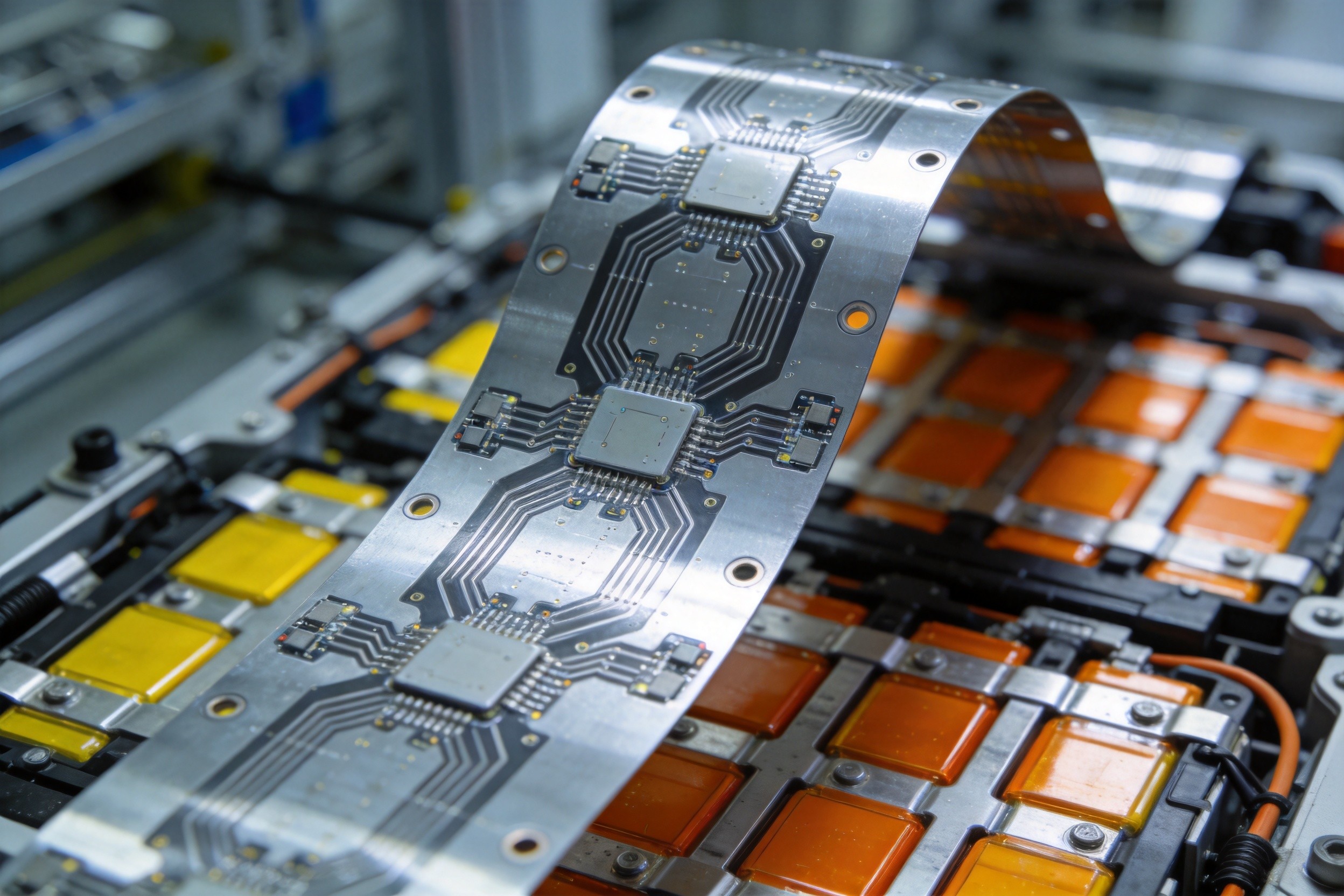
Case 1: ADAS Domain Controller — Multi-Sensor Fusion PCB
A Level 2+ ADAS domain controller integrates data from 77 GHz radar, LiDAR, and 4K cameras on a single PCB. The board must process multi-gigabit data streams (≥1 Gbps per sensor channel) while maintaining sensor synchronization accuracy within 50 μs.
PCB Design Approach: A hybrid stack-up combining Rogers RO4350B in the RF radar section (achieved insertion loss of 1.2 dB per 5 cm at 77 GHz, versus 3 dB on FR-4) with high-Tg FR-4 (Isola IS410) in the digital processing section. Differential impedance is controlled to 50Ω ±2% for radar lines (0.18 mm trace width, 0.12 mm spacing) and 100Ω ±2% for Ethernet/LiDAR lines. A clock-tree distribution network radiates from the board center, with each clock branch length-matched to within 0.3 mm, achieving sensor synchronization jitter below 35 μs. ANSYS HFSS electromagnetic simulation verified that cross-channel crosstalk remained below −70 dB.
Result: AEB (Automatic Emergency Braking) response latency reduced from 120 ms to 60 ms, with radar detection range restored to 195 m—meeting ISO 22178 safety margins.
Case 2: EV Battery Management System — Flex PCB in Harsh Environments
A BMS for an 800 V lithium-ion battery pack must monitor 108 cell voltages (millivolt accuracy) and temperatures across a physically complex, three-dimensional cell arrangement. Rigid PCBs cannot conform to the cylindrical and pouch cell geometries.
PCB Design Approach: A 4-layer flexible PCB using adhesiveless polyimide substrate (Tg > 300°C, UL 94 V-0) with rolled-annealed copper for dynamic bending reliability. Voltage sensing traces use controlled 50Ω impedance with guard traces. ZIF connectors rated to 125°C provide module-to-module interconnection. Conformal coating protects exposed areas from electrolyte exposure and humidity. The flex circuit withstands 100,000+ dynamic bend cycles at a 6 mm radius per IPC-2223C.
Result: Cell voltage measurement accuracy of ±2 mV across the full −40°C to +125°C operating range, with zero open-circuit failures after 3000 thermal cycles (−40°C to +125°C) per AEC-Q100 Rev H.
Case 3: Powertrain ECU — Thermal Management in the Engine Compartment
An engine-mounted ECU controlling fuel injection and ignition timing must operate continuously at ambient temperatures up to 150°C, with internal power MOSFETs dissipating 150 W during peak load.
PCB Design Approach: A 6-layer board using 2.5 oz (89 μm) inner copper and 3 oz (105 μm) outer copper for current carrying and thermal spreading—reducing temperature rise by 42% versus standard 1 oz copper per IPC-2152. Via-in-pad thermal arrays (0.3 mm minimum diameter, 1.2 mm maximum pitch) under the MOSFET drain pads use copper-filled vias to achieve a junction-to-PCB thermal resistance of ≤1.2 K/W. The board substrate is Isola IS410 (Tg = 180°C), and all solder joints use SAC305+Ni alloy with IMC thickness controlled to 1–3 μm for optimal fatigue resistance.
Result: Junction temperature maintained at 142°C at 150 W dissipation (within the 175°C SiC device safe operating area), with solder joint crack rate below 0.5% after 1500 thermal cycles.
Future Development Trends
AEC-Q100 Rev H and the 10-Year Life Model
The 2025 revision of AEC-Q100 has introduced accelerated life testing models that explicitly target 10-year/200,000-km durability. The thermal cycling requirement has increased to 1500 cycles, and a new combined “vibration + temperature” test simulates the simultaneous mechanical and thermal stresses of real-world driving. ISO 16750-4:2026 has also been updated with cyclic salt-spray testing (240 hours, including humidity–salt-spray–drying cycles) for 800 V high-voltage components in EVs. Timeframe: These requirements are already in effect for new qualifications starting in 2026; existing designs must be re-qualified within 18–24 months.
Centralized Domain and Zonal Architectures
The automotive E/E architecture is transitioning from distributed ECUs (50–100 per vehicle) to centralized domain controllers and zonal architectures (5–10 high-performance computers). This consolidation dramatically increases PCB density, layer count (12–24 layers), and the need for hybrid stack-ups combining RF, high-speed digital, and power sections on a single board. Automotive Ethernet (1000BASE-T1, 10GBASE-T1) and PCIe interfaces are becoming standard on ADAS PCBs, demanding signal integrity expertise comparable to data center design. Timeframe: Domain controllers are in production now; zonal architectures will dominate new vehicle platforms by 2028–2030.
ISO 26262 Third Edition and AI/ML Safety
The forthcoming third edition of ISO 26262 (expected 2027) will address the safety of AI and machine-learning-based systems for the first time, including requirements for training-data integrity, model verification, and runtime monitoring. For PCB design, this implies additional sensor-fusion processing capacity, redundant inference pathways, and hardware-level monitoring of AI accelerator health—further increasing board complexity and reinforcing the need for functional-safety-aware layout practices. Timeframe: Draft provisions are under discussion; formal adoption is expected in 2027 with a 2–3 year transition period for the industry.
Conclusion
Automotive electronics PCB design exists in a regulatory environment where reliability is not aspirational but mandatory. The AEC-Q and ISO 26262 frameworks define quantitative thresholds that every material selection, every via placement, and every solder joint must satisfy. As vehicles evolve toward software-defined, electrically propelled, and autonomously driven platforms, the PCB is no longer a passive interconnect—it is the physical infrastructure of safety. For electronics manufacturers entering the automotive supply chain, compliance is the entry ticket, but engineering excellence—demonstrated through robust thermal design, meticulous impedance control, and verifiable functional safety—is what separates suppliers who thrive from those who are replaced.
Need automotive-qualified PCB manufacturing? Connect with our team to discuss IATF 16949-certified production capabilities and AEC-Q-compliant design support.
 English
  简体中文
简体中文  Español
  العربية